Debugging the Memory Board, pt 1.
Posted on Sun 07 February 2021 in MUPS16
In which nothing works
The memory board was part of the collection of boards that arrived all the way back in August last year, and which I put together soon after, but which I never got around to properly testing. I got a little distracted by experimenting with writing a MUPS16 LLVM backend, and then work and lockdowns somehow ate up most of my time. Well, this weekend I finally got time to look, and start testing it.
The first signs weren't great. I plugged the board into the backplane, knocked up a def file for the testing shell, and tried writing a single byte to address 0x00, and reading it back again. On the plus side, this was a really good use for the macro support that I added to the shell a while ago, letting me write simple read_byte and write_byte macros that encompassed the whole sequence of control-line settings needed to read and write ram:
read_byte:
    description: read a single byte. Address given must be physical
    params:
        - physaddr
    commands:
        - set_mode data=Input physaddr=Output
        - set byte=0 memwr=1 memrd=0 physaddr=$physaddr
        - ret={get data}
        - 'print "{addr:#8x}: {data:#3x}" addr=$physaddr data=$ret'
        - set byte=1 memrd=1

write_byte:
    description: write a single byte. Address given must be physical
    params:
        - physaddr
        - byte
    commands:
        - set byte=0 physaddr=$physaddr data=$byte
        - set_mode data=Output physaddr=Output
        - set clk=1 clk2=1 memwr=0 memrd=1
        - set clk=0 clk2=0
        - set clk=1 clk2=1 memwr=1
        - read_byte $physaddr
The downside was that...they didn't work. It looked like everything was happening correctly (at least, the correct LEDs were lighting up, and probing with a multimeter seemed to show the right voltages on the input lines), but values written weren't sticking. I'm always a little reluctant to crack out the logic probe, mainly because it always feels like it takes quite a while to get everything set up, and probably because I know it usually presages a long few hours of debugging. This time I didn't waste too much time with the multimeter before bowing to the inevitable, and got the patient into the surgery, ready for some diagnosis:
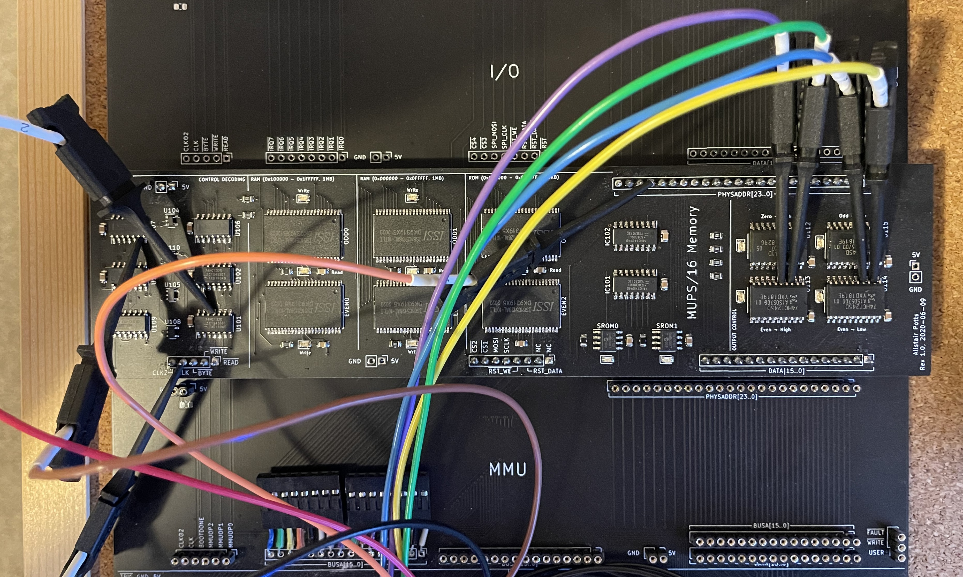
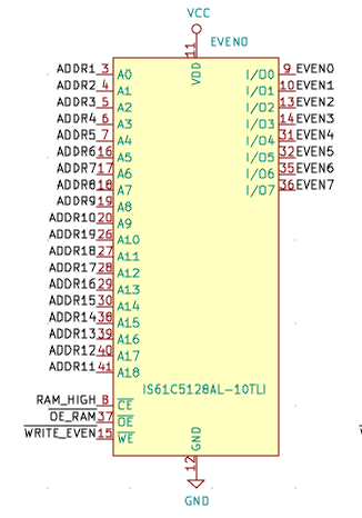
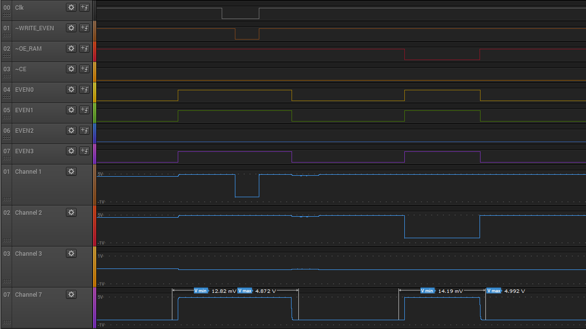
This is wired up to watch the RAM chip that should hold even addresses in the range 0x000000-0x0FFFFFFF. This chip has three control inputs: CE, which needs to be low for the chip to do anything, OE, which controls whether it outputs the byte addressed by the address inputs onto its data lines, and WE, which must be driven low then returned high while the data and address lines are kept stable to write a byte to memory. These are wired up as:
The first test was just to write a byte to address zero, and read it back. I wrote the value 0xB, and read it back. The first (write) half of the trace actually looked pretty good:
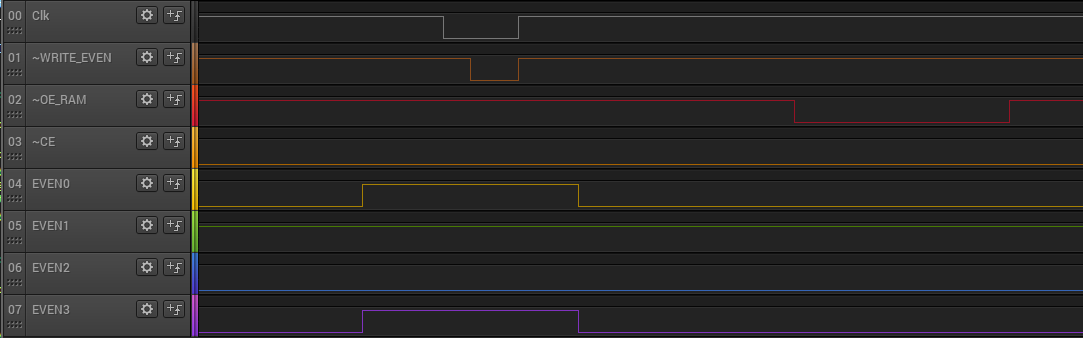
CE remains low the entire time, so the chip should be enabled. The WRITE_EVEN line is the WE on the chip, and it seems to get driven low, then back high while the values EVEN0 - EVEN4 (the bottom four bits of the input data) hold the correct value (0b1011). So far, so good. The problem seems to be in the second half, when OE_RAM gets driven low, which should prompt the chip to output the stored value back to the EVEN lines. As you can see, clearly, that doesn't happen.
I spent quite a while trying to see why this might be, and I'll skip over my floundering efforts, but in the end what made the penny drop was enabling analogue sampling on the probe:
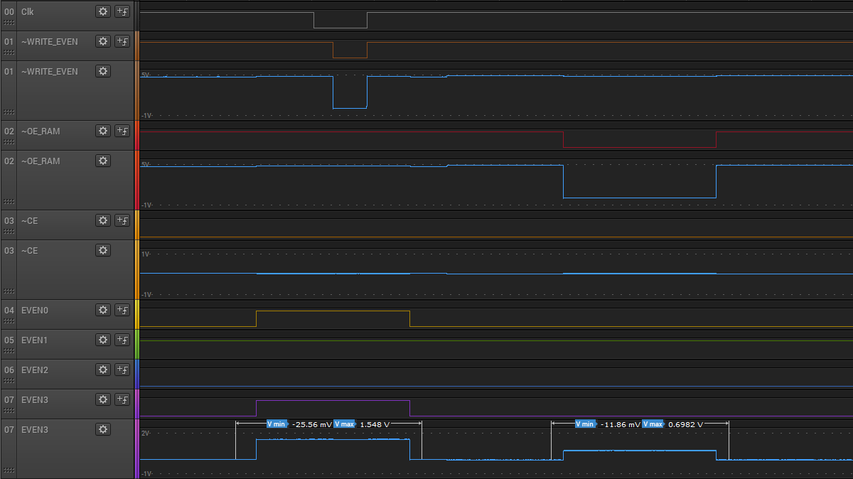
Here, we can pretty clearly see a problem. The voltages on the EVEN lines are completely wrong. I've annotated the EVEN3 line to make it a bit clearer. Even during the write, when we're setting the line high, the voltage only goes up to 1.5V, well below the level for a logical 1 that we'd expect (and well below the RAM chip's 2.2V minimum for a HIGH input). Despite this, it appears that the write did succeed, at least partially: during the read attempt it looks like the RAM chip is trying to output a 1 on the EVEN3 line (I didn't sample the voltage on the EVEN0 line). The voltage is way too low, though (barely 0.7 volts).
Unexpectedly low voltages like this always seem to be because I've got more than one device trying to drive a shared line, and this turned out to be no exception. A bit of staring at the schematic reminded me that the reset circuitry on the memory board (the small section which is only active during the reset sequence, and which help copy the serial ROM chips into RAM) can drive the data lines, if it's not disabled correctly. When I put together the def file for the board I'd left the rst_data line as an input, which means that the control board was letting it float, and it had obviously floated low, which caused the shift registers outputs to turn on. This was trying to pull the data lines low, and causing the unexpectedly low voltages. A stupid mistake.
With this fixed (by simply setting the reset-related lines to outputs, and setting them appropriately to disable them), I got a much better trace:
And now, writing and reading values back works! Tomorrow I'll try writing a comprehensive test to write and read random addresses continually, and make sure that it really does all work.