Memory
The memory unit holds the system RAM and ROM, along with their associated address decoding logic.
The MUPS/16 architecture is big-endian, and uses a 24-bit physical address space, which is logically partitioned as:
| Start | End | Size | Mapping |
|---|---|---|---|
| 0x000000 | 0x7FFFFF | 8MB | RAM |
| 0x800000 | 0x81FFFF | 128KB | ROM |
| 0x900000 | 0xFFFFFF | 7MB | Memory-mapped devices |
In reality, the sweet spot for capacity, speed and price tradeoff for SRAM chips seems to be about 512Kb, so the memory board only contains 2MB of RAM (there was enough room for 4 chips).
Memory can be either byte- or word-addressed, so reads and writes can be either 8- or 16-bits wide. Word reads or writes must be aligned to a word boundary (i.e. an even address), though this isn't enforced by the memory unit, which relies on the MMU to detect these when mapping virtual addresses. In theory I could have used 16-bit wide SRAM chips, but these are significantly more expensive than the more normal 8-bit ones. In order to be able to support both 8- and 16-bit wide operations the memory board uses separate chips for odd and even addresses. For example, if the string Hello world! were stored in RAM at address 0x0 then this would stored physically as:
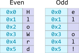
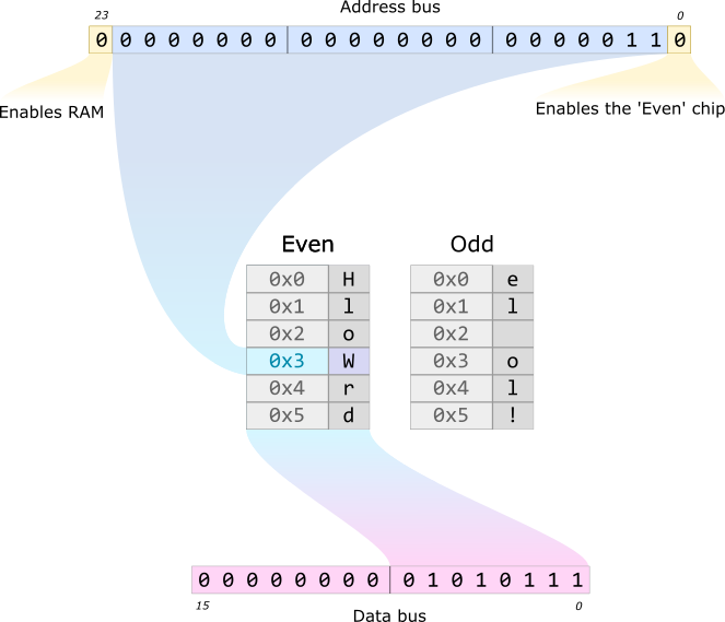
The address decoding logic can then use the combination of read/write width (byte or word) and the lowest bit of the address to decide which combination of SRAM chips to enable.
For exmaple, a byte read of address 0x6 would result in 0x0057 (ASCII W is 0x57) being output to the data bus:
A word read of the same address would result in 0x576e (ASCII W in the high byte, ASCII o in the low, since it's big-endian):
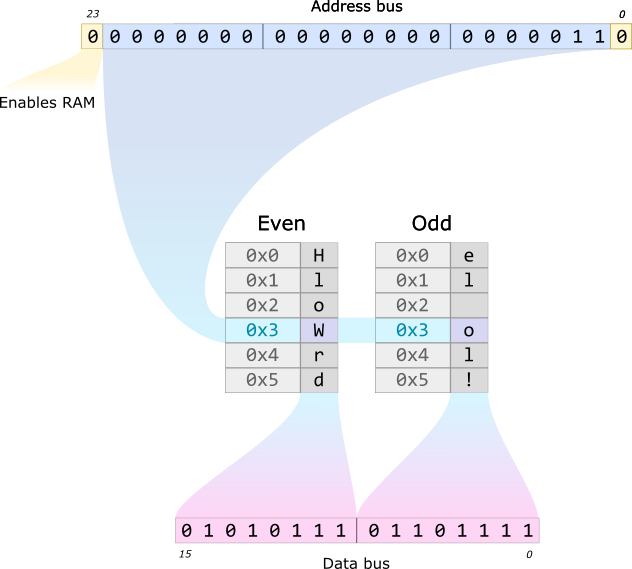
Decoding the addresses and control lines is pretty straightforward. The only slight complication is that, as you can see in the diagrams above, sometimes the even chip will be writing to the high byte of the data bus, sometimes to the low, and if we're doing a byte read then we need to output a constant zero on the high byte. In addition, when we're writing to RAM then we need the same connections but in reverse. This was implemented with a set of four 74HCT245 bidirectional bus drivers, controlled as follows:
| Connection | Enable condition |
|---|---|
| Even-High | BYTE is high |
| Odd-Low | BYTE is high or address is odd |
| Even-Low | BYTE is low and address is even |
| Zero-High | BYTE is low and address is even |
Each of the first three has their direction pin wired to WRITE, so that they transfer signals from the bus to memory on a write, and from memory to the bus on a read. The Zero-High chip is actually unidirectional, since it doesn't make sense to write to a constant (and would in fact simply be shorting the bus directly to ground, which would be bad).
Implementation
The memory board is a four-layer PCB with the same 20×5cm dimensions as all the boards that fit on the memory backplane.

The board is designed around a pair of internal buses, one for the even half of memory, one for the odd:
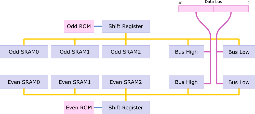
The center of the board contains six 61-64C5128AL SRAM chips, holding 512KB each. The leftmost four hold the data in the RAM part of the address space. This is split into two even-odd pairs, as described above: the first pair holds addresses 0x000000-0x0FFFFF, the second holds 0x100000-0x1FFFFF, which gets us to the combined total of 2MB. I could have used a single pair of 1MB chips, but the 512KB ones were much easier to find and quite a bit cheaper, too. The low/high split is trivial to implement, too, since we can just use bit 20 of the physical address to switch between the low and high pairs.
To the right of the four RAM chips is the ROM section. This consists of another pair of SRAM chips, a pair of 74HCT4094 shift registers, and a pair of 64KB 25LC512 serial ROM chips. On startup the reset circuit generates the appropriate SPI signals to get the ROM chips to stream their contents out on the MISO line that connect them to their shift registers, as well as incrementing PHYSADDR and setting MEMWR low every 8 clocks. Once the reset sequence finishes the shift registers set their outputs to a high-impedance state, releasing the internal buses for normal operation. The result is that immediately after power-on or reset the contents of the two serial ROM chips are copied into the rightmost pair of SRAM chips, which can then be addressed exactly the same way as RAM. The main advantage of this approach over using a pair of dedicated parallel ROM chips in sockets is that it's trivial to reprogram the serial ROM chips in place, since they don't need high voltages or exact timings. There's a header on the left-most edge of the board where an Arduino can be hooked up to flash the ROM chips (and, since the SROM chips aren't used after startup, the ROM can be flashed while the system is running). At some point I'd like to put together a simple SPI IO board for the CPU that would allow it to flash its own ROM, just for fun.
The rightmost part of the board holds the four bus drivers, configured to route the four possible combinations of even, odd, high and low to and from the data bus, as described in the table above.
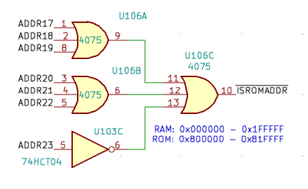
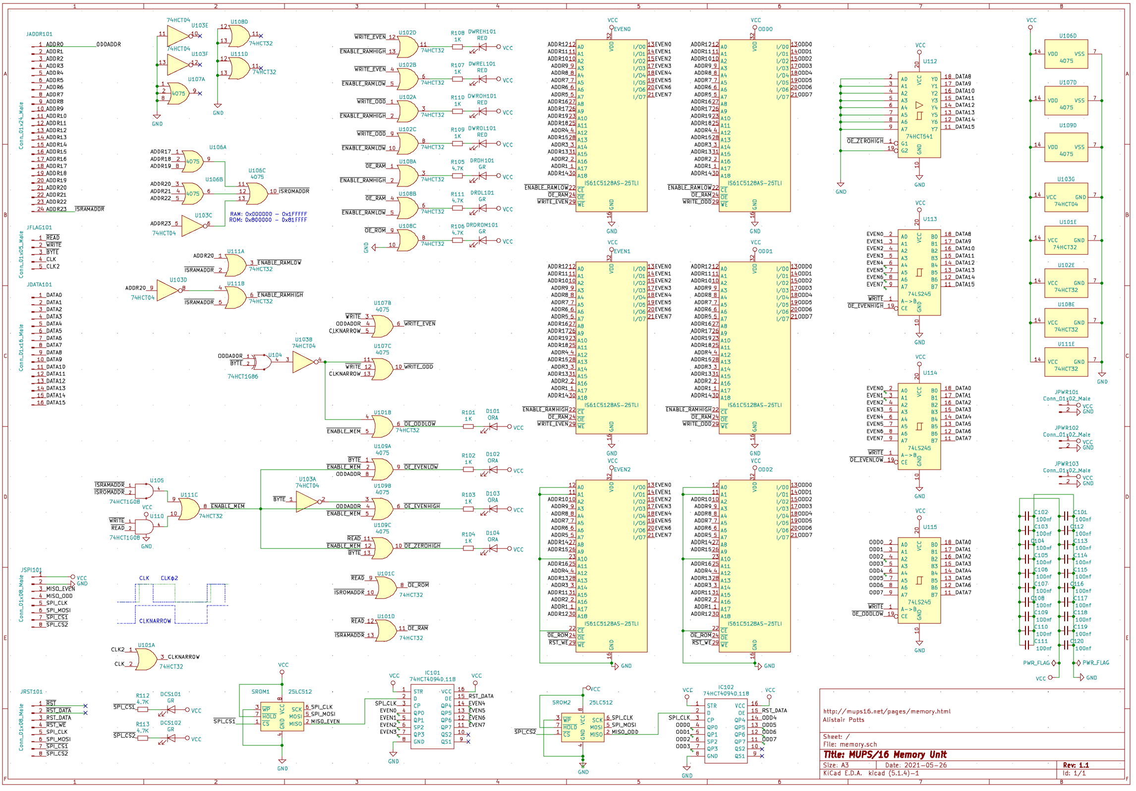
Finally, at the left is the address decoding logic. The main function of this section is to set the enable and write lines for each RAM chip appropriately, depending on the control signals MEMRD and MEMWR, and the current PHYSADDR. First, we need to detect whether the current address falls into either the RAM or ROM parts of the address space. RAM is utterly trivial: since the whole lower 8MB is considered RAM, we can just use PHYSADDR23 directly as the ISRAMADDR line:

ROM is slightly more complicated: an address is in the ROM range if the top bit (PHYSADDR23) is high, and PHYSADDR17-PHYSADDR22 are all low. This can be done with a single inverter and a 74HCT4075 triple 3-input OR gate:
The remainder of the logic is largely just a collection of OR gates to selectively enable the various RAM chips based on whether the address is even or odd, MEMBYTE is low, etc. The full schematic looks like:
This is also available as a PDF.