Register Unit
Overview
The MUPS/16 CPU has 16 registers in total, each 16-bit, but because the instruction encoding only
has 3 bits for the source and destination registers only the first 8 registers are addressable in
most instructions. The upper 8 are system registers, and can only be manipulated by certain
instructions (in particular, the mfs and mts instructions, which move values between the lower
and upper registers).
The 8 user registers are:
| Index | Mnemonic | Description |
|---|---|---|
| 0 | r0 |
Zero register. Always zero, no matter what value is written to it |
| 1-4 | r1-r4 |
General-purpose user registers |
| 5 | sp |
Stack pointer |
| 6 | r5 |
General-purpose user register |
| 7 | ra |
Return address register. Return address is saved in this register by jal and jalr instructions |
The 8 system registers are:
| Index | Mnemonic | Description |
|---|---|---|
| 8 | spc |
Saved PC. The pc register is copied to this register before a trap handler is invoked |
| 9-11 | s1-s3 |
Used to transfer arguments to trap handlers, and to pass arguments to the rfe instruction |
| 12 | tsp |
Task state pointer. Has no architectural significance, but intended to hold a pointer to a memory area in which current process state can be saved on a trap |
| 13 | tmp |
Temporary register. Used by the CPU to hold intermediate results in some instructions |
| 14 | pc |
Program counter. Contains the address of the next instruction to execute |
| 15 | flg |
State flags. Used to hold the privilege level (user or system), whether the boot process is complete, and the current IRQ mask |
The odd split between r1-r4 and r5 is an artifact of the original design, which had pc as a
user-addressable register at index 5 (and indeed, the PCB for the register board still shows that).
When the PC was made into a system register on the control board (so that it could auto-increment
without needing the ALU) it freed up a slot for another general-purpose register.
Implementation Details
The register file is implemented on two boards. Registers 0 to 13 are on the register boards, which is made up of 4 major parts:
- control-signal decoding logic
- reset logic, to initialise all registers to zero
- some single-byte and sign-extension logic (used when loading a single byte from memory into a register)
- the flipflops and output drivers for each of the 14 registers
The pc and flg registers are separate, and implemented in the control unit, as they need extra
connections for their inputs and outputs.
There are four buses in the main register board: the external data input bus and A and B
output buses, and an internal bus. The reset and sign extension units drive the internal data bus,
and all registers read their content from it. The sign extension unit is the only part that actually
reads the external data bus, and either passes the data through to the internal bus or modifies it
as necessary.
Overall schematic
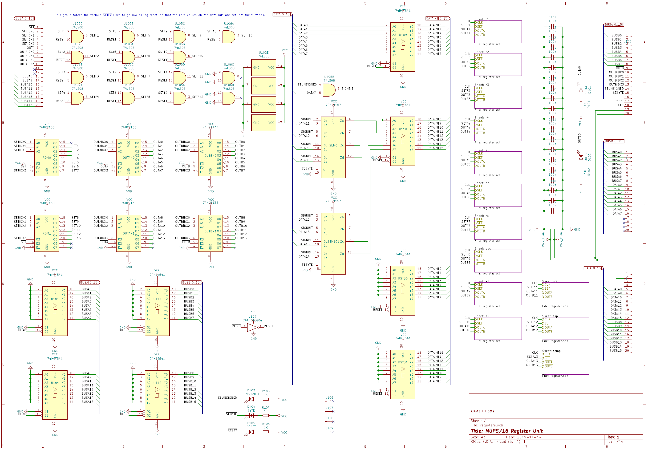
There is also a PDF of this image, and the original Kicad schematic file will be put on Github once I've fixed the known problems.
Control signal decoding logic
The register unit has 17 control lines:
~SET: active-low signal. If low, causes the register with the index given in the fourSETIDXlines to latch a new value on the next clock.~OUTA: active-low signal. If low, causes the register with the index given in the fourOUTAIDXlines to output their value to theAbus.~OUTB: same as above, for theBbus.~SEBYTE: active-low signal. If low, causes only the lower 8 bits of the data bus to be used on the next latch. The contents of the upper 8 bits is determined by the~SEUNSIGNEDsignal.~SEUNSIGNED: active-low signal. If this is low, and~SEBYTEis low, then the upper 8 bits latched on the next clock cycle will all be zero. If high, then sign-extension is done from bit 7 of the data bus.~RESET: active-low signal. If low, causes all the registers'SETsignals to go low, and also asserts all zeros onto the internal data bus. This will cause all registers to reset to zero on the next clock cycle.
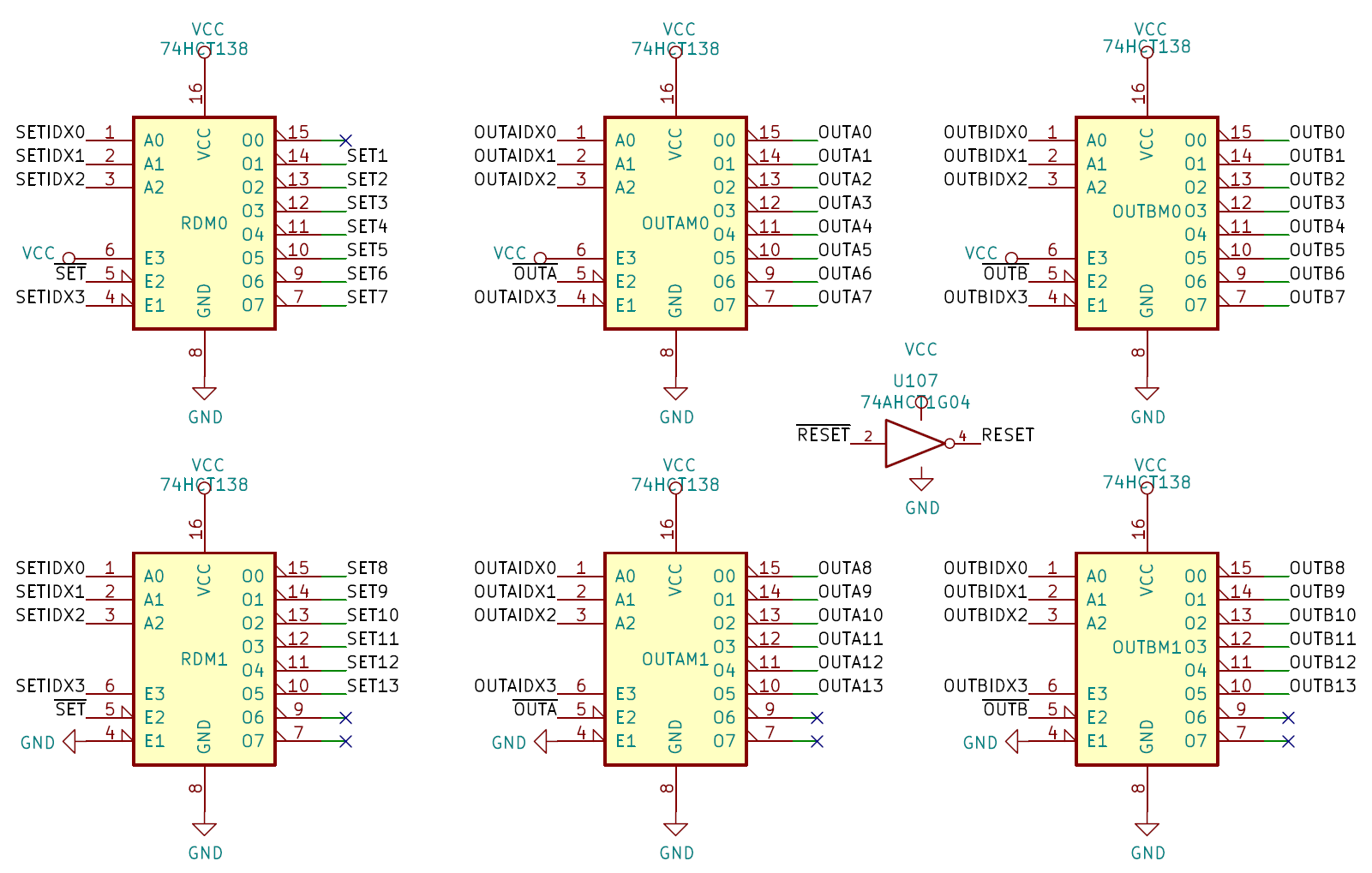
This is fairly simple logic. Most of the work here is in deciding which registers should have their
~SET, ~OUTA or ~OUTB lines set. Each of these lines is active-low (the naming is misleading on
the schematic, as I didn't indicate that they were active-low. I may go back and fix that).
Since we have 14 registers, we have 14 output lines for each of the three signals.
As each of the set/outa/outb indices is a 4-bit value the logical solution would be to use a 4-16
demultiplexer, but I couldn't find any of these in the HCT logic series. Fortunately, however, the
74HCT138 3-8 demultiplexer has a nice feature that makes it trivial to chain two together to
make a single 4-16 decoder: each 138 chip has 3 separate enable lines, two of which are active-low
and one of which is active-high. If any of the three is not set then the chip will output high on
all outputs, regardless of the value of the select bits. The truth table looks something like:
| E1 | ~E2 | ~E3 | S0 | S1 | S2 | Output |
|---|---|---|---|---|---|---|
L |
X | X | X | X | X | HHHHHHHH |
| X | H |
X | X | X | X | HHHHHHHH |
| X | X | H |
X | X | X | HHHHHHHH |
H |
L |
L |
L |
L |
L |
LHHHHHHH |
H |
L |
L |
H |
L |
L |
HLHHHHHH |
H |
L |
L |
L |
H |
L |
HHLHHHHH |
H |
L |
L |
H |
H |
L |
HHHLHHHH |
etc.
Since our outputs are all active-low this means that if any of the enable lines are disabled all the outputs will be off.
To chain two demultiplexers together we simply connect the 4th bit of the select lines to ~E3 on
the first chip, and to E1 on the second. If the input index is between 0 and 7 then bit 4 will be
zero, and the first demux is active to output low on one of the output lines 0-7, while the second
demux is 'inactive', and will output high on outputs 8-15. If the input index is between 8 and 15
then bit 4 will be high, and we get high on outputs 0-7 and low on one of 8-15.
We also take advantage of one of the remaining unused enable lines on each chip to handle the
overall ~SET, ~OUTA and ~OUTB lines. By wiring the appropriate line to ~E2 on both 138
chips in a pair, we can ensure that the demuxes do not output low on any output line unless the
overall signal is low (asserted).
There is also a solitary NOT gate here, to provide an inverted RESET signal. We use this inverted
value in the sign-extension unit below.
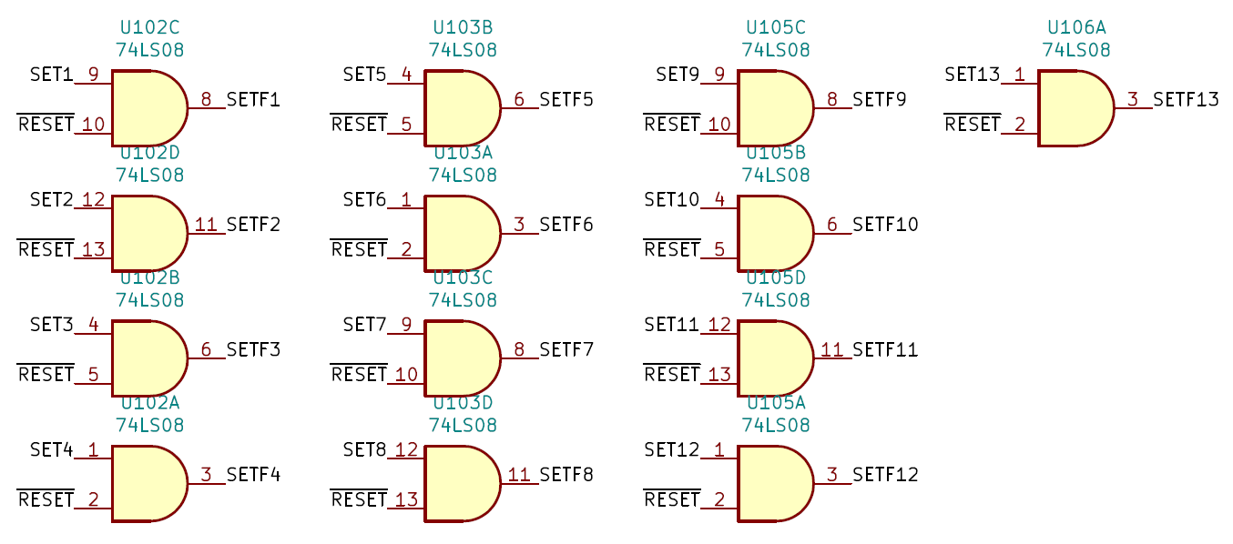
Reset logic
When the register unit is first powered on it, each register will hold random values. This is a
particular problem for the PC register, as we don't really want to start executing at a random
address. We use the reset logic here to ensure that all registers can be set to zero by setting
~RESET low and pulsing the clock.
The first part of the reset logic works by setting all registers' ~SET lines low if the ~RESET
signal is low. We do that by simply ANDing each of the ~SETx outputs from the control decoding
logic above with the ~RESET signal:
The second part of reset logic ensures that the internal data bus is set to zero while ~RESET is
low. We do this with a pair of 74HCT541 line drivers, each of which has all its inputs tied to
GND, and ~RESET wired to its active-low G2 input:
Note that there's an obvious optimisation here, which I probably should have taken: we don't really
need to zero out all registers on a reset. We could have just zero'ed out the PC register, and
let software take care of setting the other registers before they're used. This would have saved 4
74HCT08 chips (we could just use a pair of the tiny 74HCT1G08 chips, one for the ~SETF6 signal
and one for sign-extension).
Sign extension logic
The sign extension logic is fairly simple:
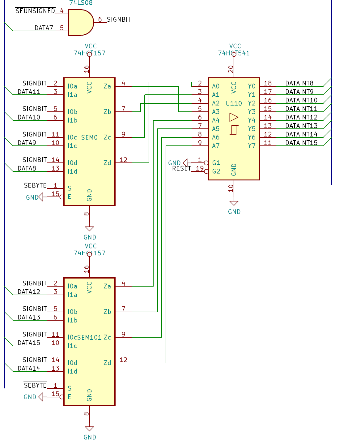
The byte and sign-extension logic only potentially affects the upper 8 bits of the values off the
data bus, and sign-extension is only done if ~SEBYTE is low. This is implemented by having a pair
of quad 2-1 74HCT157 multiplexers, with the ~SEBYTE line connected to the select line of each.
This has the effect of either passing the input value off the data bus through if ~SEBYTE is
high, or outputting the sign bit otherwise.
The sign bit is computed simply by ANDing together the ~SEUNSIGNED line and bit 7 from the data
bus. If ~SEUNSIGNED is low (asserted) then the sign bit will always be zero; if it is high then
the value of bit 7 is used as the sign bit.
The last part of this unit is a 74HCT541 line driver, which is there to ensure that we don't
attempt to drive the internal data bus at the same time as the reset logic is doing so. The output
of the two 157 multiplexers is fed through the line driver, which is enabled by the inverted reset
signal, so that it drives the bus only when the reset unit isn't doing so.
I'm not 100% sure that the byte and sign-extension logic really belongs in the register unit: there will also be some sign extension needed on immediate value output from the control unit, so perhaps it would have been better to have a dedicated sign extension unit, but for now it's here.
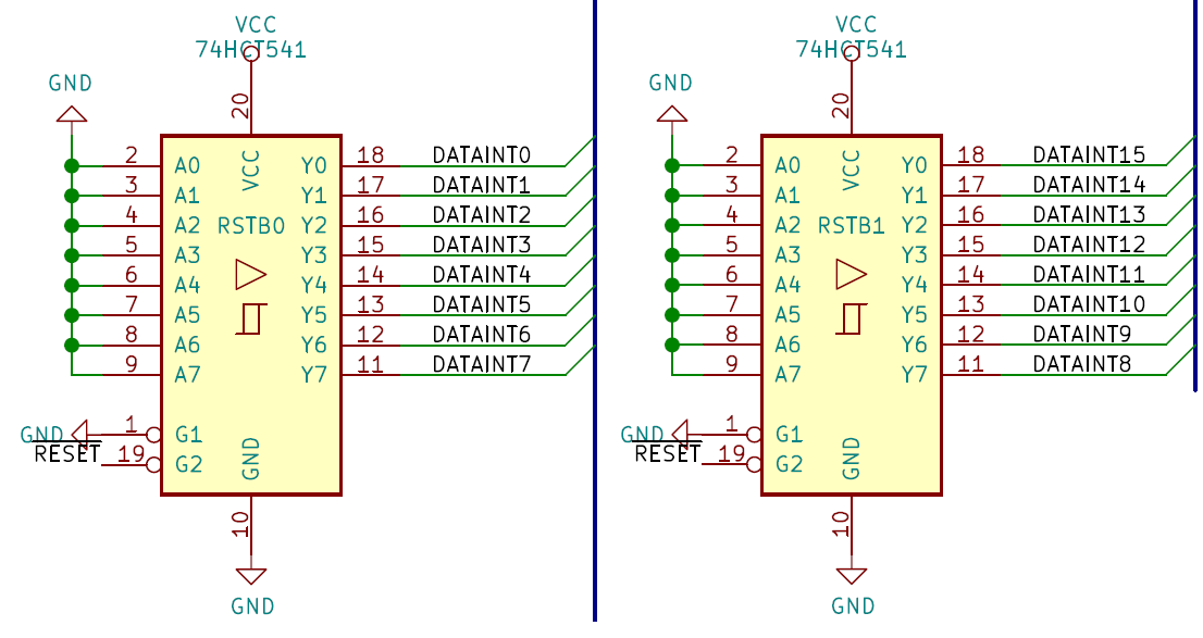
Flipflops and output drivers
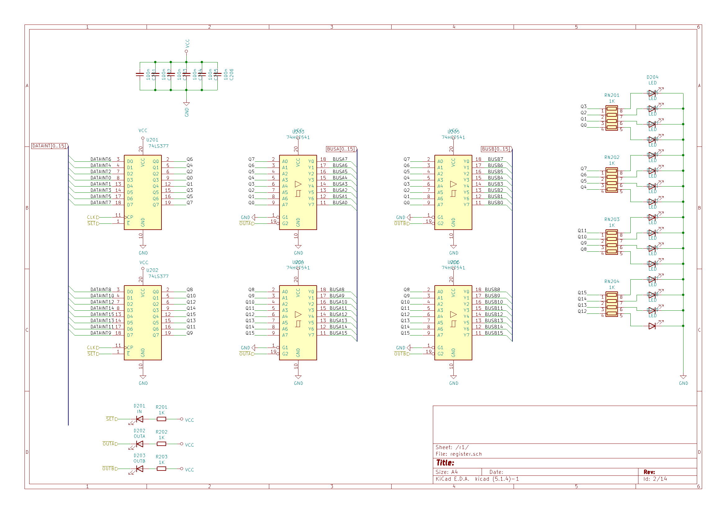
PDF of this image.
This is the guts of the whole register unit. Each register consists of a pair of 8-bit 74HCT377
flipflops, and four 74HCT541 bus output drivers. These are grouped into one set of three chips for
the low 8 bits and another for the high 8 bits, which simplified the PCB layout significantly.
Each flipflop is connected to the relevant bits of the internal data bus. The 377 chips do not have
tri-state outputs, so their output is directly connected to two line drivers, each driving either
the A or B buses.
Each register has three control lines:
- a
SETline to control whether they latch a new value on the next clock. - an
OUTAandOUTBline that controls whether the line drivers should drive the relevant bus, or remain in a high-impedance state.
Since the flipflops are always outputting they are also directly connected to 8 LEDs, to diplay their contents. The LEDs used here are low-power, high-brightness green Wurtz diodes. I was a little concerned that driving these directly from the flipflops might cause problems, but so far it doesn't seem to have done. The LED current is limited by 4.7KΩ resistors, in neat little 4-unit resistor networks.
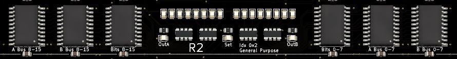
PCB layout
The PCB is a two-layer, 300mm by 150mm board, with a ground fill on the bottom layer. I could have made it slightly smaller, but I liked the nice round numbers of these dimensions, and it should make sizing the remaining boards in the CPU easier. I would love to have gone to 4 layers for this, as it would have massively simplified routing (getting power and ground everywhere it was needed made the signal traces far more complicated than I'd like), but the cost of a 4-layer board this large was prohibitive.
Routing was done by hand; I didn't even try using an auto-router for this. Since there is a lot of repetition in the layout I used the excellent replicate layout plugin. With this I could lay out a single register as I wanted it and then duplicate the layout for the other 12 registers. The only restriction was that the process of updating the other registers after a change would clobber any other traces or silkscreening that fell within the bounding rectangle containing all the components for the dependent registers. This meant that I had to have the layout of the registers pretty much perfect before adding the long top-to-bottom traces carrying the buses and control lines. In practice this wasn't a major problem, and given how much time the plugin saved me, a very minor inconvenience.
Problems
As this was only the second PCB I've ever designed I'm fully expecting the design to have issues, especially considering the length of some of the traces and the incomplete ground fill, but thus far testing has gone pretty well. There are three problems that I know of so far:
- I accidentally swapped lines 14 and 15 of the
databus on the input to the sign extension multiplexer, so those two bits are swapped when reading data. Fortunately, since this isn't an internal connection I can work around this by swapping the wires connecting those lines to the externaldatabus. - More seriously, there's a transient(ish) issue with bit 11 getting stuck on when reading, affecting all registers. This is almost certainly down to my shoddy soldering, rather than a design problem, but I've not nailed it down yet. I suspect a bad joint that's leaving an input to one of the register output multiplexers floating somewhere.
- There's also a cosmetic error in the silk-screen layer, with the four multiplexers at the top
that control the output lines for each register incorrectly labelled as
SET DECODING.