MMU
Overview
The MMU has three jobs in the MUPS/16 processor:
- to map between the 16-bit virtual addresses that processes use and the 24-bit physical addresses that the memory and IO units use;
- to provide separation between process address spaces, so that each process can treat memory as if it owned all bytes between 0 and 65,535, without worrying about other processes (or even being able to see their memory);
- to provide protection of some addresses within a process' address space, so that some addresses can be marked as read-only, or as accessible only to the OS.
To do this, the MMU implements a basic paging scheme, dividing the virtual address space up into 256 pages of 256 bytes each, with each virtual page able to be mapped to any of 65,536 physical pages, giving a total addressable memory size of 16Mb.
Mapping a page takes a single cycle, with the mapped address available for outputting to the physical address bus on the second cycle of an instruction. As well as virtual to physical address mapping the MMU supports two different permission levels on a page (system and user), and supports a writable permission bit that must be set when a memory write is performed. If either of these permission constraints is violated, or if an attempt is made to map a page that has no page table entry, then a page fault is raised to the exception unit.
Paging
The basic idea of a page-based virtual memory is that both the pysical and virtual address spaces are divided up into some number of equal-sized pages (that's over-simplifying a little, as most modern CPUs do support multiple page sizes, but in simple implementations, including this one, pages are fixed size). An address can therefore be viewed as the combination of a page number and an offset within that page:

When we want to convert between a virtual address (as seen by the process), and a physical address (as seen by the memory hardware) we take the virtual page and apply some transformation that uses some combination of the virtual page number and a process identifier to produce a physical page number. The final physical address is then that physical page number combined with the original offset. If we took the pair of addresses in the diagram above as being the virtual and physical address in a mapping, the virtual page 0x05 was transformed into physical page 0x0732, and the low 8 bits (the offset) passed through unchanged.
In most implementations of virtual memory the virtual address space is much larger than the physical one. The MUPS/16 is the opposite: each process can only access 64KB of memory, even though RAM is so cheap that the design allows for up to 8MB of physcial RAM. In addition, since I designed the system to use memory-mapping for all IO each process has to sacrifice some of its precious address space to map in IO pages. This is why I ended up using such a small page size of 256 bytes, to minimise wastage.
On the plus side, the small 16-bit virtual memory space of the MUPS/16 allows us to make the MMU hardware fairly simple, as individual page tables never get very large. In most modern CPU designs the MMU hardware cannot maintain the full page table for a process in memory at once. A 64-bit Intel or AMD processor uses a 48-bit virtual address space, and with the default 4KB page size they would require 236 table entries per process, which is unfeasible. They therefore have to implement a dynamic page table cache, in which the MMU maintains a subset of the page table entries in memory at any one time, with hardware to detect cache misses and raise an exception to the OS.
With the much smaller 64KB address space of a 16-bit process, however, it's perfectly feasible to keep the whole page table in memory at once. In fact, given that the smallest easily available SRAM chips are 8KB, even with tiny 256-byte pages it's possible to keep 32 full page tables in memory at once.
Each page table entry is 19 bits long: 16 bits for the physical page address, and three status bits:
- mapped, set to 1 if the entry is valid
- system, set to 1 if the page can only be accessed when the USER flag is not set, indicating that the current process is running in supervisor mode
- writable, set to 1 if writes to the page should be allowed
I used 3 parallel IS61C64AL-10TLI 8k×8 SRAM chips, giving the MMU the ability to hold a total of 8192 entries of 24 bits each. The upper 5 bits of each entry are unused at the moment.
Since we have enough room to store 32 full page tables simultaneously, there is also a register which holds a 5-bit value indicating the index of the currently-active page table. When we want to look up an entry in the page table we combine the 5 register bits with the virtual page index (the top 8 bits of the virtual address) to form a 13-bit address, which is then passed to the address lines of the SRAM chips. The low 16 bits of the result become the upper 16 bits of the physical address, with the low 8 bits of the virtual address passing through unchanged:
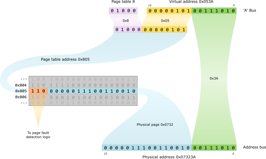
This approach is a little wasteful in memory space if most processes don't use the maximum 64KB of memory, as there will be a lot of unmapped page entries, but, as well as being simple, it means that process switches can be very fast, as we can switch the entire page table by simply changing the table register (assuming we have fewer than 32 processes running at once. If we have more then the OS would have to do more work). The downside is that setting up a process is slightly slower, as the OS has to set all 256 entries for the new process, even if most are unmapped, as there's no hardware support for clearing the mapped bit on multiple pages simultaneously.
Boot Mode
The mapping process described above suffers from an obvious bootstrapping problem: on startup the table RAM will have random values, and so can't be used to map addresses. To enable the CPU to access memory safely during this initial period the MMU has a second mode that's active whenever the BOOTDONE line is low (which is guaranteed to be the case on power on or reset). In this mode no mapping at all happens, and the full 16-bit virtual address passes through unchanged. The upper 8 bits of the 24-bit physical address are set to 0x80. For example, if the same 0x053a virtual address as above were mapped in boot mode, the result would be:
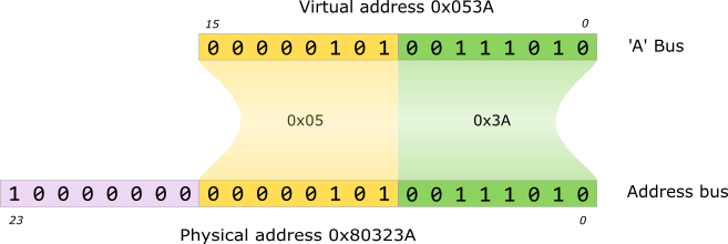
This boot mode has the result of mapping all memory accesses to the first half of ROM (0x800000-0x80FFFF). The code in the first few bytes of ROM can then set up a barebones page table that maps in some code pages from ROM and basic stack, and set the BOOTDONE flag to enable MMU mapping.
Page Faults
When a mapping operation is performed, the three permission bits read from the resulting page table entry are checked against the current flags and the operation being performed, and a page fault is raised (the FAULT line goes low) if any of the checks fail.
The three possible failures are:
- no mapping: there is no page mapped at the virtual address, indicated by the mapped bit in the entry being 0
- write violation: a write operation is being performed, but the mapped page does not have the writable bit set
- protection violation: the mapped page has the system bit set, but the USER flag is 1
Because the FAULT line is produced by simple combinational logic from the table contents it may transiently go low as the RAM addresses and outputs settle (as described below). For this reason, the control unit must latch the FAULT line at the end of the cycle.
No page faults will be raised if the MMU is running in boot mode, as the page table isn't used in this mode.
Address Output
The full address-mapping process takes two clock cycles. The actual mapping as described above completes within a single cycle, but the resulting 24-bit physical address is not output it to the PHYSADDR bus immediately. Instead, at the end of the cycle the address is latched into three 74HCT574 8-bit latches. During the next clock cycle the control unit will instruct the MMU to output the address mapped on the previous cycle. There are a couple of reasons for this:
- in my initial design, the ALU was used to calculate PC+2 in the first cycle of each instruction, and since the ALU outputs to the DATA bus, as does the memory unit, they can't both be active at the same time. This meant that there was no point trying to do a map + read in one cycle;
- more importantly, it takes some amount time for the physical address to stabilise during the mapping: not all bits of the page table address calculation will change at exactly the same time, and the RAM chips themselves specify that the maximum time for the outputs to stabilise after the address has finished changing is 10ns, during which the output of the RAM is not defined. If we fed the RAM output directly onto the PHYSADDR bus then the physical address would be unstable for some time at the start of the cycle. This isn't good: if we were mapping an address to perform a write then the MEMWRITE control line might be low while the address is still unstable, which would lead to a write to random addresses. Even during reads it's unacceptable (imagine a memory-mapped IO device that buffers data in a FIFO queue: a spurious read could result in it deciding the data had been consumed, and popping it from the queue).
By buffering the data and only outputting it on the second cycle we can ensure that it is completely stable throughout the cycle.
Note that this two-step mapping process means that we need two MEMWRITE control lines: one that is passed to the MMU during the mapping cycle, so that it can detect write violations, and a second that's passed to memory the next cycle during the actual write. We cannot use the same signal directly, as this would cause the memory unit to write during the mapping cycle, when neither the data nor the address are ready yet.
Control and Setup
The operation of the MMU is controlled by the 3-bit MMUOP line. This gives 8 possible operations the MMU can perform:
| Value | Operation |
|---|---|
| 0 | Map address: take contents of A bus, map to a physical address, and latch result |
| 1 | Output mapped address: output the address computed in the previous cycle to the PHYSADDR bus |
| 2 | Output table entry low word: output the low 16 bits (i.e. physical page) of the table entry whose address is read from the A bus to the DATA bus |
| 3 | Output table entry high word: output the high 8 bits (i.e. permission bits) of the table entry whose address is read from the A bus to the DATA bus. In the high word of the DATA bus, output the contents of the table index register |
| 4 | Output fault address: output the address that was being mapped when the most recent page fault occurred to the DATA bus |
| 5 | Set table index register: set the contents of the table index register from the bottom 5 bits of the A bus. Corresponds to the PTSI instruction |
| 6 | Set table entry: set the table entry at the page table address read from the bottom 13 bits of the A bus. The 16-bit physical page number is read from the B bus, and the 3 permission bits are read from the top 3 bits of the A bus. Corresponds to the PTSE instruction |
| 7 | Nothing: the MMU is idle |
Note that the 'set table entry' operation requires that the full page table address be given on the A bus; it is not combined with the index register in any way. This is so that the OS can set the table entry for any process, not just the current one.
Implementation
The MMU is a four-layer PCB with the same 20×5cm dimensions as all the boards that fit on the memory backplane.

Control decoding
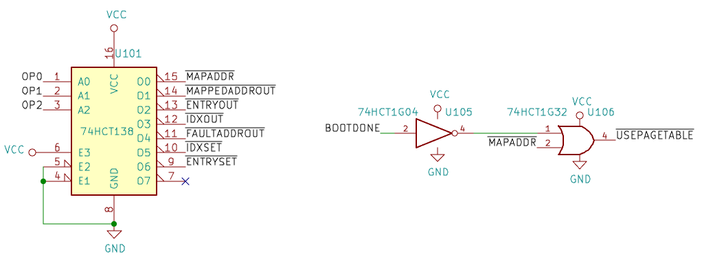
This is very simple: just a 74HCT138 3-8 line demux to select the operation, and a USEPAGETABLE line that's only low if we're mapping an address and BOOTDONE is set (i.e. we're not in boot mode any more).
Page table address calculation
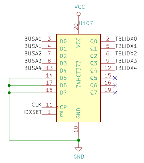
First, we have the index register itself. This is just a 74HCT377 8-bit synchronous register with an enable line, which is set iff the IDXSET operation is selected.
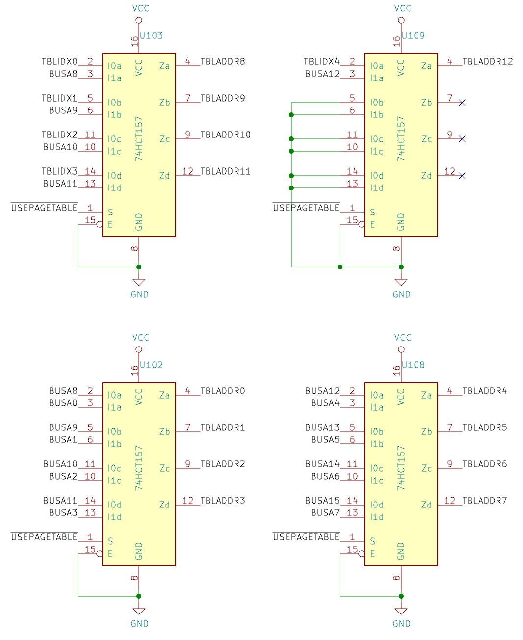
The remainder of the address construction is four 74HCT157 2-1 multiplexers. These switch between two different address outputs:
- if we're performing a mapping operation then USEPAGETABLE will be low, and we combine the 5 bits from the index register with the low 8 bits of A (the virtual page number) to get the address
- otherwise, all other operations that need to access the page table (set table entry, read table entry low/high) take the address directly from the low 13 bits of the A bus
Page table RAM
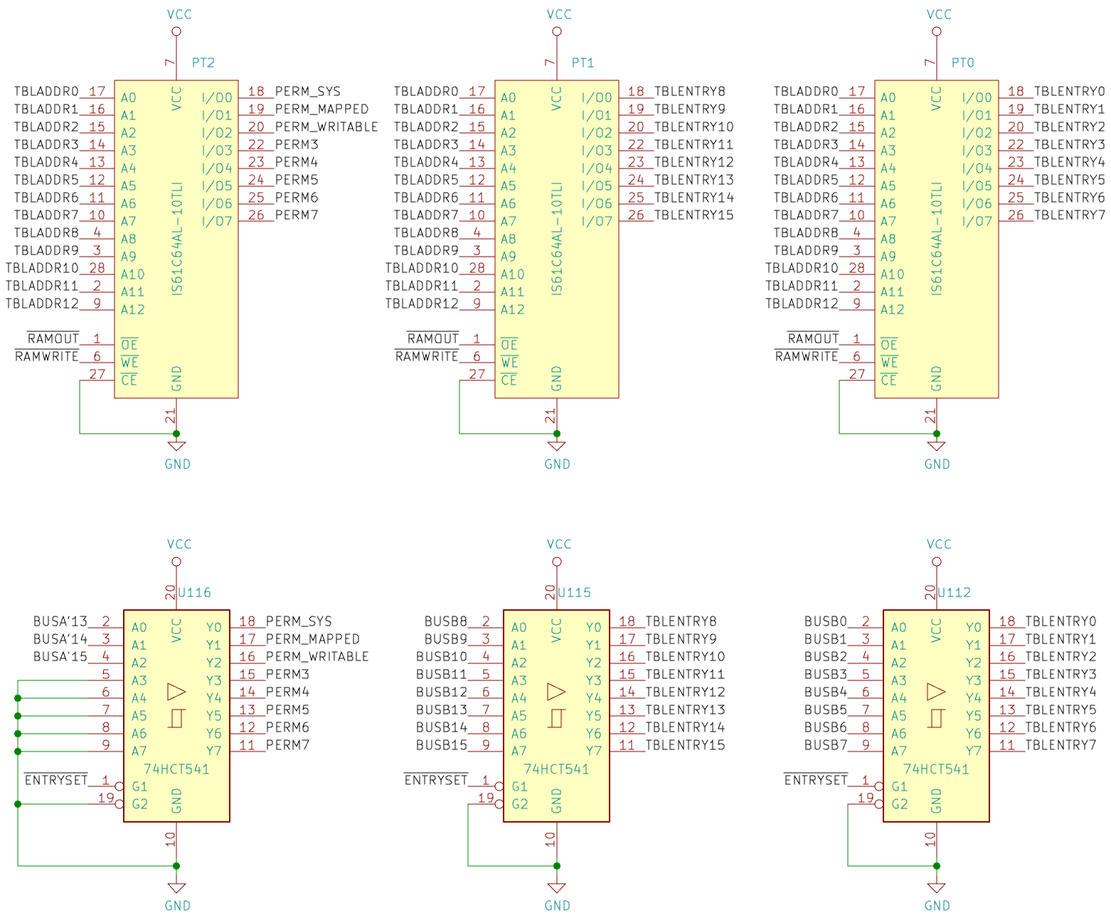
The page tables themselves consist of three IS61C64AL-10TLI SRAM chips. The 13 address lines are connected to the output of the multiplexers described above. The data lines are, as is normal in most RAM, used for both input and output. The RAMOUT and RAMWRITE signals (described below) control whether we're reading from or writing to the RAM (or neither, in which case the output is in a high-Z state). The three 74HCT541 buffers are used to connect the B bus to the RAM IO pins when we want to write to the table RAM, during a 'set table entry' operation (ENTRYSET is low).

Constructing the RAMOUT/RAMWR signals is straightforward. The operations are encoded so that the first four operations are all the ones that need the table RAM to output. This means that we can directly use OP2 as RAMOUT, since it will be low whenever one of the first four operations is selected.
The RAMWR signal is also pretty trivial, as it's low only when the 'set table entry' operation is selected (ENTRYSET is low) and the clock is low. This ORing with the clock is so that the address lines have time to settle in the first half of the cycle before we set RAMWR, to ensure that we don't write to the wrong address.
Note that there's a slight oddity here: we don't gate on the plain CLK signal, but on a calculated CLKNARROW one. This is because the CPU has two clocks: CLK is an asymmetric pulse that's high only in the first quarter of the cycle, CLKɸ2 is a more normal pulse with a 50% duty cycle. Both clocks are synchronised, with the same period. The reason for having two clocks is to allow for circuits like the table RAM one above, where we cannot write until all inputs have settled:

Note that CLKNARROW here is completely redundant: we could just as easily have used CLKɸ2 directly. It is a vestige of an earlier clock design in which CLKɸ2 was slightly offset from CLK.
Page fault detection
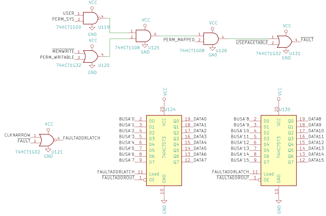
The top half of the fault circuit is simply a combinational series that checks each of the permission bits coming from the table entry against the USER and MEMWRITE inputs, and then gates the output on USEPAGETABLE, so that faults are reported only when performing a non-boot-mode mapping.
The lower part latches the fault address into a pair of 74HCT573 chips. These chips are convenient because they have 3-state outputs, so they can be connected directly the DATA bus, but the downside is that they don't have an enable input; instead, they latch their inputs whenever their LOAD line transitions from high to low. We use the CLKNARROW signal again here, combining it with FAULT and inverting it to get a signal that goes high only in the second half of a cycle, and only if FAULT is low during that second half. At the end of the cycle it will drop low again, triggering the latch. All other times the signal will stay low, leaving the last fault address latched ready to be read by the OS.
Output drivers
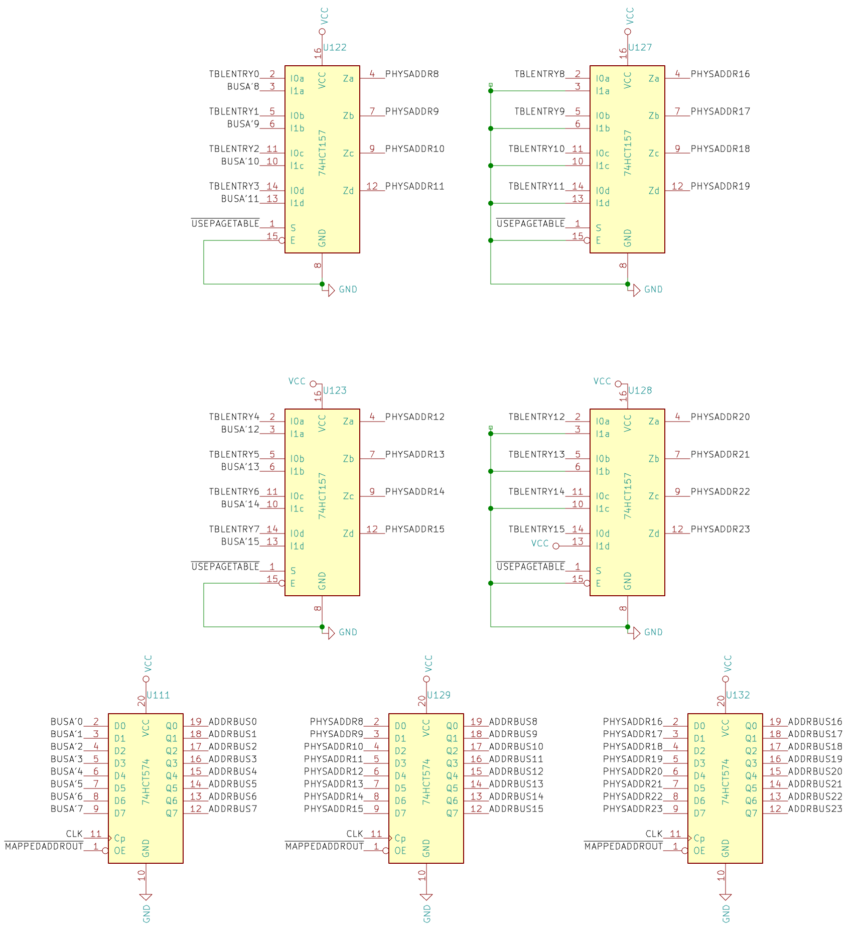
Not much interesting here. There are four 74HCT157 2-1 multiplexers to choose between the physical page output from the table RAM (normal mapping), or a constant 0x80 and the high 8 bits of the virtual address from the A bus (boot-mode mapping), with their outputs latched in four 74HCT574 flip-flops. Note that these flip-flops latch their values on every cycle, so the mapped address is only available on the cycle immediately after it was calculated.
In retrospect, I'm not sure why I used 573 chips for the page fault latches and 574 ones here. That seems a little unnecessary.
The full schematic is available as a PDF.