ALU
Overview
The MUPS/16 ALU supports 13 basic operations:
- 4 arithmetic operations:
ADD,ADDC(add with carry),SUB,SUBB(sub with borrow) - 4 logical operations:
AND,OR,XORandNOR - 3 shift operations:
SLL(shift left logical),SRL(shift right logical),SRA(shift right arithmetic) - an
EQoperation that uses thecarry_outflag to indicate whether the twoAandBinputs are equal
All operations operate on two inputs, taken from the A and B busses, and (apart from the EQ
operation) produce a single output to the data bus. It's possible to suppress output to the data
bus by setting the ~alu_out line high. This is mainly useful for comparisons, where we're
interested in the flag outputs (carry_out and less_than), not the result of the computation.
Instruction Details
| Instruction | data |
carry_out |
less_than |
Notes |
|---|---|---|---|---|
ADD |
A + B |
1 iff carry out of top bit |
undefined | |
ADDC |
A + B + carry_in |
1 iff carry out of top bit |
undefined | |
SUB |
A - B |
0 iff borrow occurred |
1 iff A < B |
|
SUBB |
A - B - 1 + carry_in |
0 iff borrow occurred |
undefined | |
AND |
A & B |
0 |
undefined | |
OR |
A | B |
0 |
undefined | |
XOR |
A ^ B |
0 |
undefined | |
NOR |
~(A | B) |
0 |
undefined | Can be used with B input set to Zero register to get ~A |
SLL |
A << B |
0 |
undefined | No shift-in or shift-out supported |
SRL |
A >> B |
0 |
undefined | No shift-in or shift-out supported |
SRA |
A >> B, with sign-extension |
0 |
undefined | No shift-in or shift-out supported |
EQ |
A - B |
1 if A == B, 0 otherwise |
undefined |
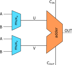
Arithmetic and logic unit
High-level design
The arithmetic and logic units are combined into a single one, using one pair of 4-way multiplexers
per bit to perform the logical operations, feeding into 4 sequential 74HCT283 4-bit adders to
handle addition and subtraction.
Being able to manipulate inputs before they go into the adder is useful for a variety of operations, as we'll see later.
Logical operations using multiplexers
The logical operations are implemented using 16 4-way multiplexers, using an idea I first saw in the
6502 CPU, and written up in detail here. In short,
though, the fundamental observation is that we can turn a 4-1 multiplexer into a programmable logical unit for a
single bit. The truth-table for a 4-1 multiplexer with inputs u, v, w, x looks like:
| Select input | Output |
|---|---|
00 |
u |
01 |
v |
10 |
w |
11 |
x |
Compare this to the canonical truth table for, say AND of two bits A and B:
B input |
A input |
Output |
|---|---|---|
| 0 | 0 | 0 |
| 0 | 1 | 0 |
| 1 | 0 | 0 |
| 1 | 1 | 1 |
If we produce the select input for the multiplexer by using a single bit from the A bus and a
single bit from the B bus, then we can produce any truth table by varying the values of u-x.
For example, to perform an AND of the input bits, we would set u=0, v=0, w=0, x=1. To get
XOR, we could set u=0, v=1, w=1, x=0. This means that we can perform any of 16 logical
operations with one multiplexers per bit. The complete set of possible operations is:
u |
v |
w |
x |
Output |
|---|---|---|---|---|
| 0 | 0 | 0 | 0 | 0 (constant zero output, regardless of inputs) |
| 0 | 0 | 0 | 1 | A & B |
| 0 | 0 | 1 | 0 | ~A & B |
| 0 | 0 | 1 | 1 | B |
| 0 | 1 | 0 | 0 | A & ~B |
| 0 | 1 | 0 | 1 | A |
| 0 | 1 | 1 | 0 | A ^ B |
| 0 | 1 | 1 | 1 | A | B |
| 1 | 0 | 0 | 0 | ~(A | B) |
| 1 | 0 | 0 | 1 | ~(A ^ B) |
| 1 | 0 | 1 | 0 | ~A |
| 1 | 0 | 1 | 1 | ~A | B |
| 1 | 1 | 0 | 0 | ~B |
| 1 | 1 | 0 | 1 | A | ~B |
| 1 | 1 | 1 | 0 | ~(A & B) |
| 1 | 1 | 1 | 1 | 1 (constant one output, regardless of inputs) |
With this, we can see how to perform the arithmetic and logical operations that the ALU supports.
ADD and ADDC
These are the simplest operations. For ADD we set the control lines for MUXu to 0101, so it passes
through A unchanged, set MUXv to 0011, so it passes through B, and set CIN to 0,
and we get A+B on the output. ADDC is the same, except we pass the CARRY_FLAG control line to
CIN.
SUB and SUBB
Since all we have is an adder, we implement A - B as A + -B. -B in two's-complement arithmetic
is just ~B + 1 (where ~B is the bitwise complement of B). We can compute ~B trivially, since
it's one of the supported operations in the multiplexers, and we can feed the +1 in by setting
CIN to 1. So, to compute SUB, we set MUXu to 0101 (pass through A), set MUXv to 1100
(~B) and set CIN to 1. For SUBB, the only change is that we pass CARRY_FLAG to CIN.
AND, OR, XOR, NOR
To compute these we only need a single set of multiplexers. Since we've set things up so that all
output will go through the adder anyway, we simply force the V input to the adder to be 0, by
setting MUXv to 0000, so that the U input passes through unchanged. The MUXu lines are just
set to the appropriate row from the table above.
EQ
This one is more interesting, and all credit goes to
/u/marcelk72 for the idea. The obvious way of determining
if A == B is to compute A - B, and test whether the result is 0. This requires dedicated
circuitry for the zero detection, which would require 5 additional ICs. Instead, we can use the
existing circuitry, and compute A ^ ~B + 1, which will result in a carry out iff A == B. To see
why, look at the truth table for A ^ ~B:
A |
B |
~B |
A ^ ~B |
|---|---|---|---|
| 0 | 0 | 1 | 1 |
| 0 | 1 | 0 | 0 |
| 1 | 0 | 1 | 0 |
| 1 | 1 | 0 | 1 |
The result is 1 iff A == B. So, if the inputs are identical, we will end up with a result of
1111111111111111. If we then add 1 to this, the carry will ripple up through all the bits and
we'll get a carry out of the result. If any bit is different, there will be at least one 0 bit in
the result, which will stop the carry from propagating, and we'll get a carry out of 0. So, for
equality detection, the control unit can set OP=EQ and test the carry out for 1.
Summary of logic/adder inputs
Putting all this together, these are the values that we need to set on the MUXu, MUXv and CIN
lines for each arithmetic or logical instruction:
| Operation | MUXu |
MUXv |
CIN |
|---|---|---|---|
| ADD | 0101 |
0011 |
0 |
| ADDC | 0101 |
0011 |
carry_in |
| SUB | 1010 |
1100 |
0 |
| SUBB | 1010 |
1100 |
carry_in |
| AND | 0001 |
0000 |
0 |
| OR | 0111 |
0000 |
0 |
| XOR | 0110 |
0000 |
0 |
| NOR | 1000 |
0000 |
0 |
| EQ | 1001 |
0000 |
1 |
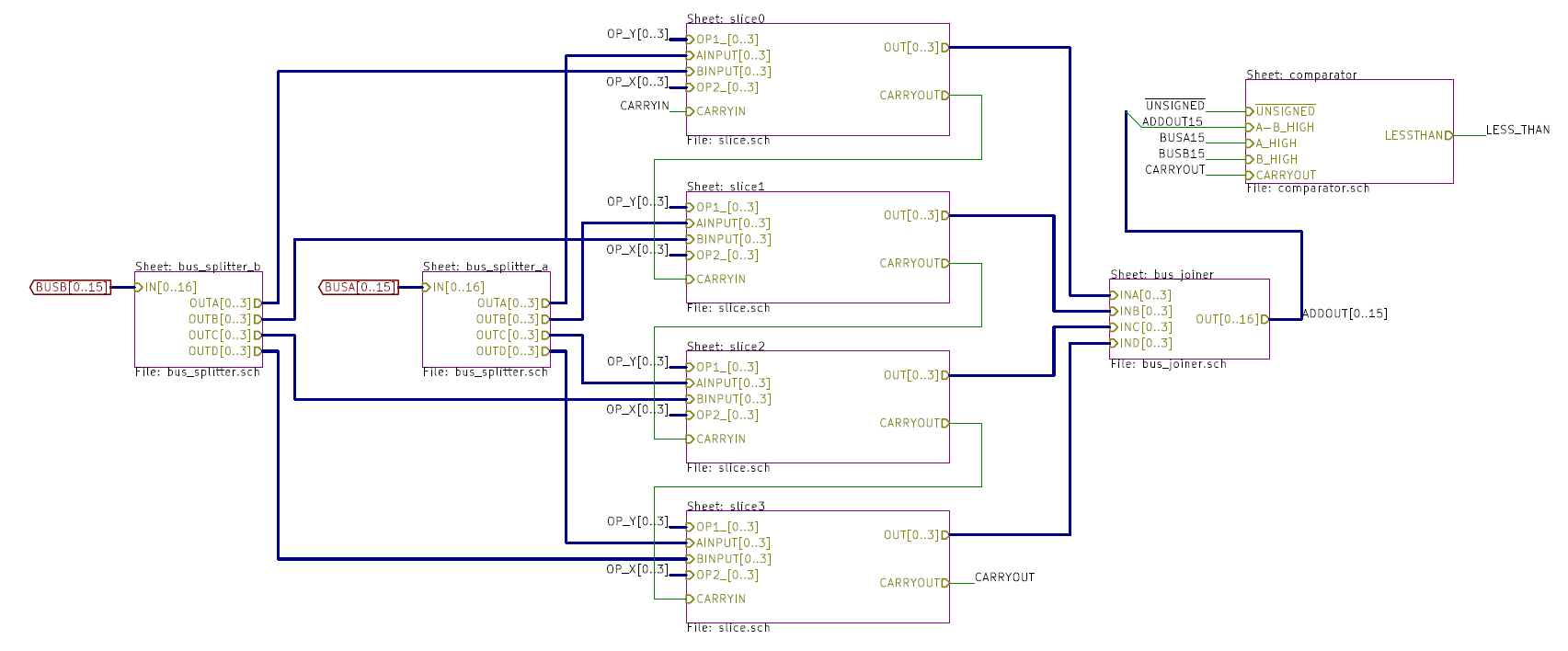
Schematics
The overall layout of the arithmetic and logic unit looks like:
Each slice looks like:
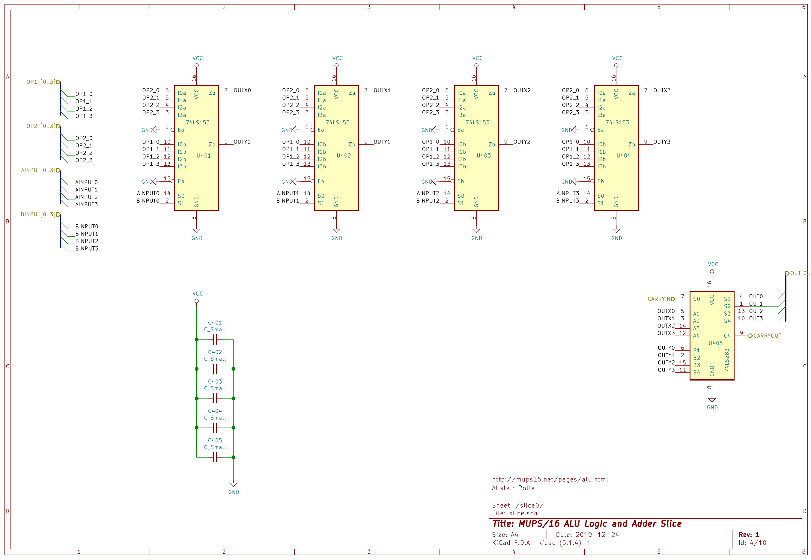
Note that there is a PDF of this image, together with all the other schematics in a single document.
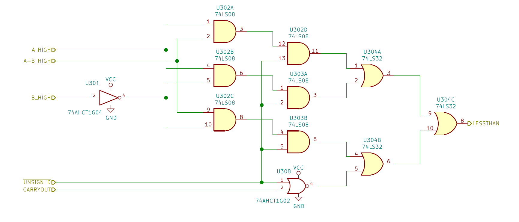
Less-than comparison
A minor operation supported by the ALU is detecting whether A < B. This isn't implemented as a
separate operation, but rather appears as an extra output line that is only significant when OP is set
to SUB.
For less-than comparison, we have to consider signed and unsigned number separately. Unsigned
comparison is very simple. If A < B, then computing A - B will result in a borrow, and so
COUT will be 0 (with subtraction, COUT of 1 means no borrowing happened, 0 means we
borrowed). Signed comparison is more complicated, as we have to consider the sign of each of the
inputs, as well as the sign of the result of the subtraction. Getting the sign of each value is
simple enough, as we can just look at the value of the top bit. The possible combinations of signs
are shown below:
A |
B |
(A-B) |
A < B? |
|---|---|---|---|
+ |
+ |
+ |
No |
+ |
+ |
- |
Yes |
+ |
- |
irrelevant | No |
- |
+ |
irrelevant | Yes |
- |
- |
+ |
No |
- |
- |
- |
Yes |
The following circuitry implements the comparison:
Shift unit
High-level design
The shifter is built from has 4 layers of multiplexers, responsible for shifting by 1, 2, 4 and 8 bits respectively. Each layer can switch between on, in which case it outputs its input shifted by an appropriate amount, or off, when it simply passes through its input unchanged. This way we can build up any shift amount from 0..15 by toggling layers. For example, to shift by 9 we would set layers shift1 and shift8 to on, and leave shift2 and shift4 off.
As an illustration, the following shows a very cut-down shifter with only 4 bits, and hence two layers, capable of shifting any amount from 0 to 3 bits.
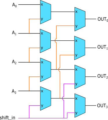
You can see how if we set the the first layer of multiplexers to use their x input, then they will
just pass through their output unchanged. If we set them to use their y input, however, then the
output of that layer will be SHIFT_IN A3 A2 A1, which has shifted the input right by one bit.
When shifting, we need to decide what to shift into the top bits here. We could decide to shift in
the values that are being shifted out of the bottom bits, which would give us bit rotation, but here
I've gone for simply shifting in a constant bit, repeated as many times as necessary. Normally, this
SHIFT_IN bit will be 0, as this matches the semantics you expect from simple bit-shifting. The
only time it will be 1 is if we're doing an SRA operation (arithmetic right shift), in which case
SHIFT_IN will be whatever the value of the high bit in the input is.
We could implement left- and right-shifting separately, using two sets of four layers each, and a final
layer of multiplexers to choose between the sets. Using the common 74HCT157 quad two-way
multiplexers, that would require 4 chips per layer, for a total of 36 chips. We can be slightly more
efficient by implementing a right shift by reversing all the input bits, doing a left shift, then
reversing the output again. We can implement this with an initial selectable reversing layer, the four
right-shift layers, and a selectable final reversing layer, for a total of 24 chips.
There remains the question of how we control each of the shifter layers. Fortunately, that's simple.
We wire up all the multiplexers so that 0 on their control line means pass through unchanged.
Then, if we assume that we want to shift the value on the A input bus by the value on the B bus, then
we can set the control line for the shift-by-1 layer to bit B0, the control line for the
shift-by-2 layer to B1, etc. The reversing layers have their control lines set to 1 iff we're
doing a right shift.
Schematic
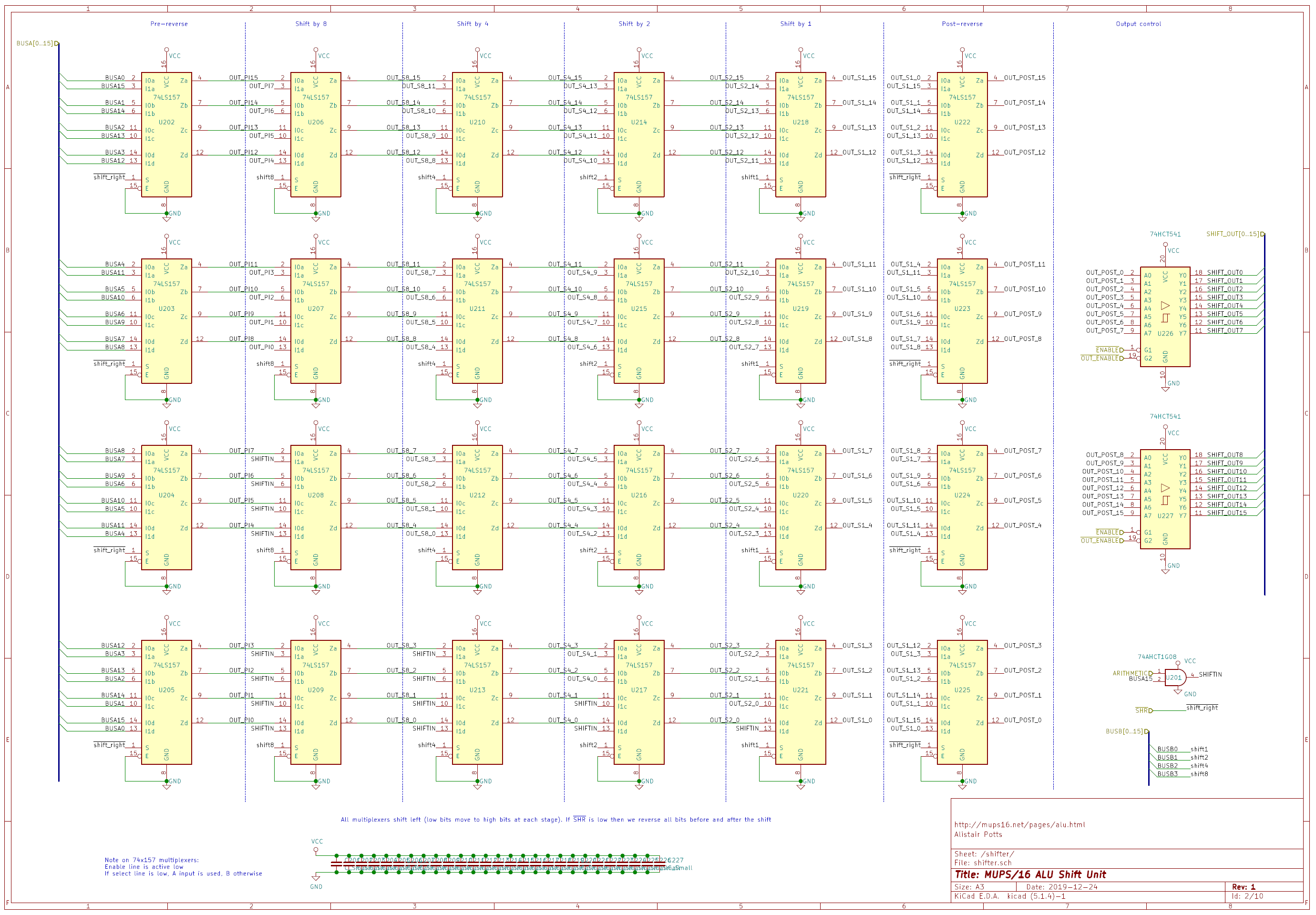
This just reflects the description of the shifter above. You can see the 6 layers of multiplexers,
along with a final pair of 74HCT541 bus drivers that allow us to control whether the shift unit
should drive the output bus.
Control signal decoding logic
The ALU has 6 control lines:
OP: 4-bit encoding of the operation to perform~OUT: active-low signal. If low, result of the operation will be asserted to thedatabusCARRY_FLAG: carry-in bit, used only inADDCandSUBBoperations
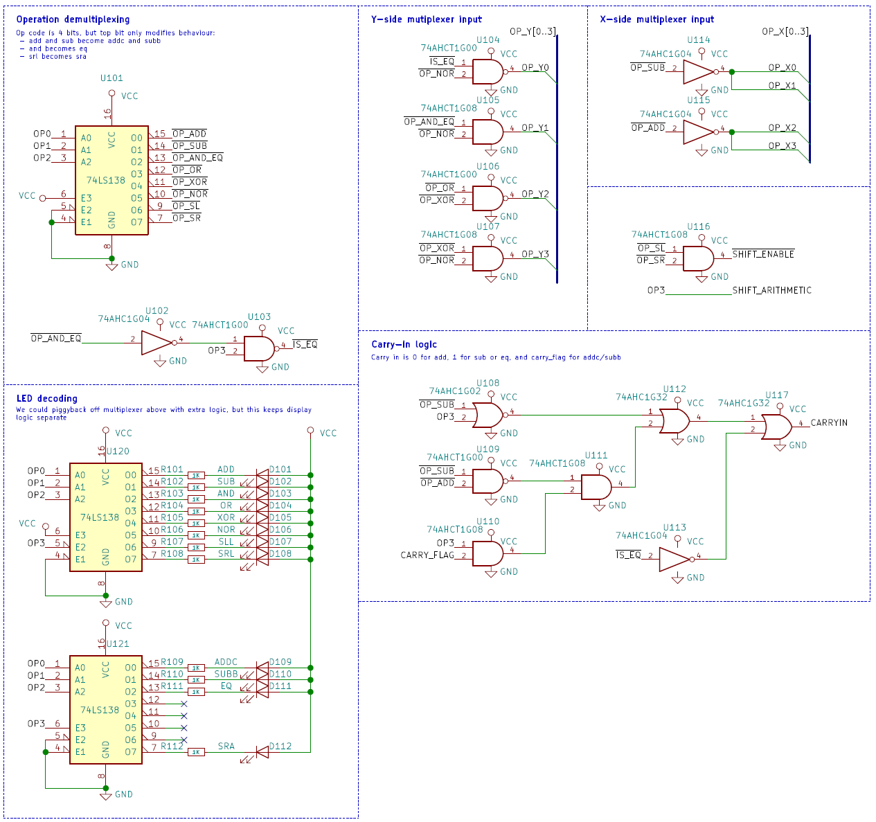
The demultiplexing of the OP lines is split into two parts: one dedicated to producing the LED outputs, for
simplicity, and a separate one for the actual decoding. Note that the real decoding only uses
the lower 8 bits: the upper bit switches between variants of the same instruction, so ADD becomes
ADDC, SUB becomes SUBB, SRL becomes SRA and AND becomes EQ.
The output of the demux
feeds into two groups of logic gates, each group producing four sets of internal control signals
that drive the multiplexers in the arithmetic/logic unit. Refer to the table above for the values
that each of the control signals should have for each operation (note that OP_Y in the schematic
corresponds to the control inputs for MUXu in the table above, and OP_X corresponds to MUXv).
The carry_in value for the adders is also computed here, based on the operation and the value of
the CARRY_FLAG input.
Thanks
Many thanks to /u/marcelk72 for his help with the equality
logic, and to /u/SaltPeppah for pointing out a bug with
subb in this writeup.