Detour: copying ROM to RAM on startup
Posted on Sat 30 May 2020 in MUPS16
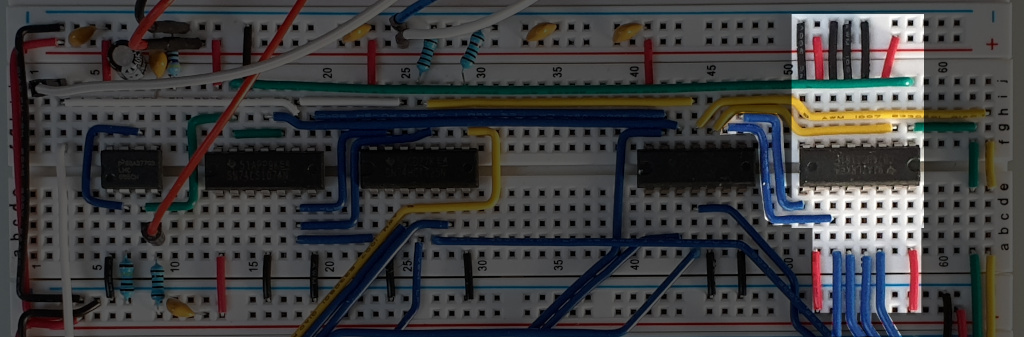
I've been toying with the idea of trying to use serial ROM chips in my build for quite a while, but I couldn't find anyone else who had done something similar, and wrote it off as too complicated. A couple of weeks ago, however, I started working on the PCB for the ROM component of the MUPS/16, and decided to have another look.
Parallel ROM chips are certainly easier to design for, but they have a few properties I really don't like:
- they're huge, compared to most surface-mount components
- reprogramming them requires removing them from the board, which forces them to be installed into a chip holder, further increasing their size.
- they're expensive (roughly £5-7 each, and I need at least 8 of them)
- they're slow; the fastest I could find that weren't hundreds of pounds had an access time of ~140ns, which is terrible compared to the ~10ns of a 50p SRAM chip. Given that every single cycle requires at least one ROM access for microcode, and we have to allow for a second memory access to ROM, this would automatically cap the clock rate at no more than about 3Mhz.
Now, admittedly #4 is unlikely to be a big issue to start with, since I'd be surprised if I could get the clock rate that high anyway, but I'd still like to give myself some wiggle room. The biggest practical objection is the difficulty of reflashing the chips, especially since microcode changes would require flashing up to 7 separate ROM chips.
Serial ROM chips are much smaller and much cheaper than parallel ROM chips, but they're obviously completely unusable for microcode (or even normal ROM) in their serial form. The ideal combo would be to have a single serial ROM chip, and copy it into multiple SRAM chips on startup. I wasn't sure if this would be practical, since I wanted to stick to my rule of having no microprocessors in my build, which precluded the obvious solution of using an ATTiny and a couple of shift registers. So, I decided to give it a go.
Most serial ROM chips these days seem to use the I2C protocol, so I started my first attempt with an I2C ROM chip. This really wasn't very successful. I2C is a reasonably complicated protocol to implement solely in discrete components. In particular, the clock-stretching and acknowledgement parts of the protocol gave me a few headaches. I got clock stretching working, but implementing acknowledgements was getting more complicated than I was comfortable with. Shortly after giving up on that, however, I found the Microchip 25LC512 ROM, which uses the SPI protocol. SPI is a much simpler protocol than I2C, and after about two weeks of sporadic evening work I had a reliable prototype working on breadboards.
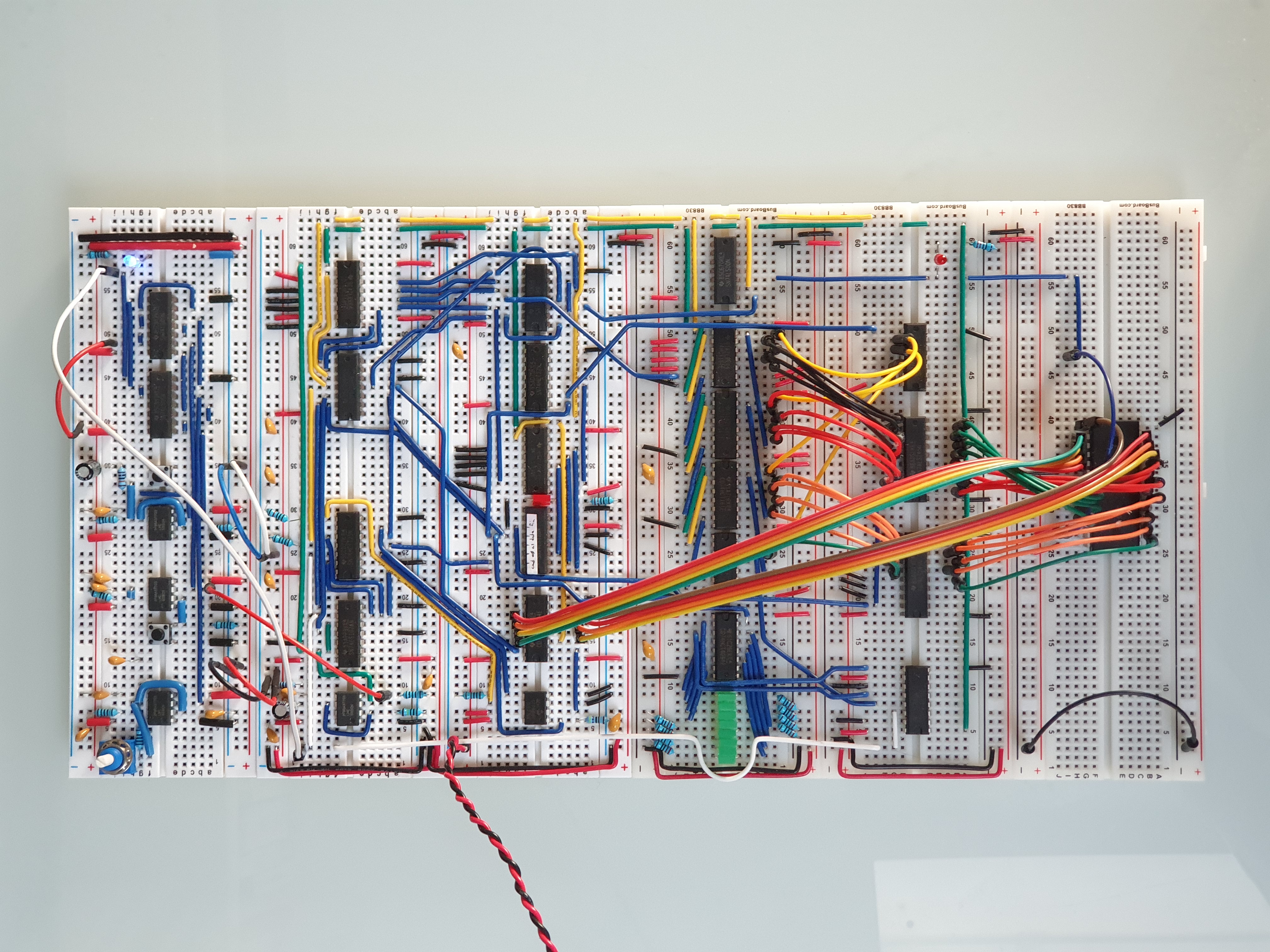
Fundamentally, what we're trying to do here is to set up a circuit such that when power is first applied to the system, we hold the rest of the system in reset mode while we copy all 64KB out of the serial ROM into one or more SRAM chips, and once that's done, release the reset line and allow the system to boot.
To get an idea of what we need to do, we can look at the example read sequence from the ROM chip's datasheet:
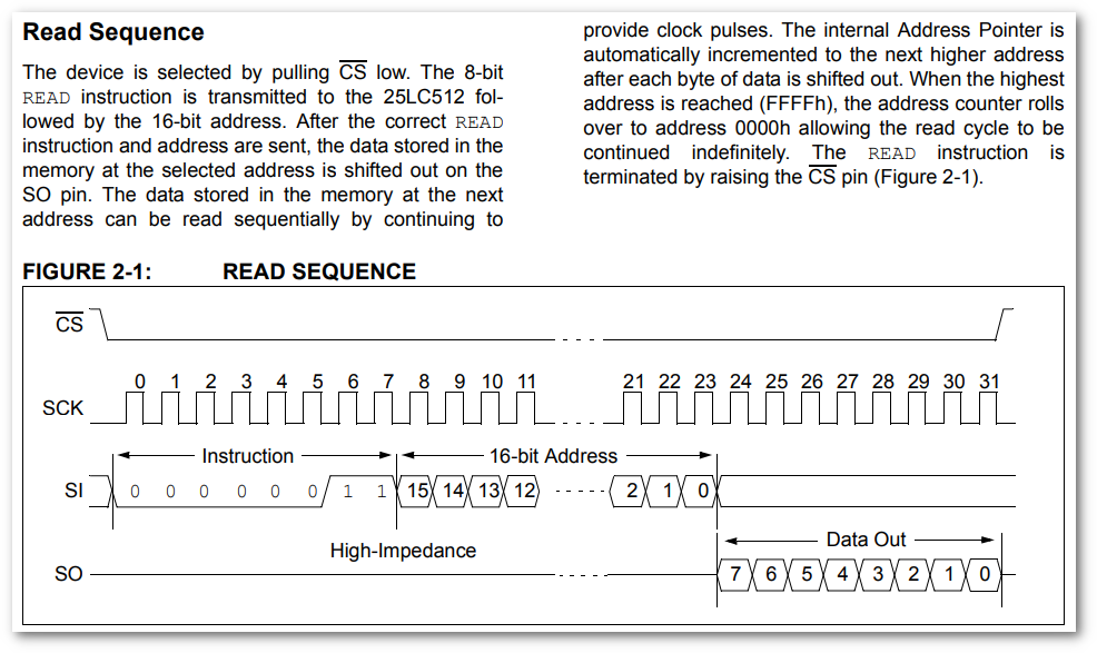
Looking at this, we can see that we're going to need, at minimum:
- a clock
- some kind of flipflop for the
CSline - a counter for individual bits
- a counter for bytes
- a shift register to hold the bytes coming out of the ROM chip
It turns out that it's much simpler to implement if we split the byte counter into two layers, with a state counter, which will have 5 states:
- command, in which we send the
READcommand (00000011); - addr0, in which we send the first byte of the address (always 0, for our use-case);
- addr1, in which we send the second byte of the address (also always 0);
- data, in which we read 65,536 bytes of data from the
MISOline and send it to RAM; and - finished, in which we set
CShigh again and stop the SPI clock
and a separate address counter, which will count from 0 to 216-1 once we hit the data state.
Power-on reset
We're using a few stateful components (the flip-flop and counters), so we need to make sure that they're all initialiased to a sensible value on powerup. We do this with a simple one-shot 555 timer circuit that stays low for a short time after startup, then goes high. This is connected to the green wires, which extend around the board to reach all the components that need resetting on startup.
Since we're going to be triggering the CS line off
this, we also want to make sure that we syncronise the
reset line with the clock, so that it goes high on a
clock boundary. We do this with a JK flip-flop (we only really need a simple SR latch, but I had an
SN74LS107 chip handy, so I used that). We wire
the CLR line of the flipflop to reset, so that the state is initialised to 0 on startup,
and we set J to 1 and K to 0, so that the latch is set on the first clock pulse after reset goes
high.
Note that the J and K lines aren't directly wired to 1 and 0, since we want to be able to clear
the flipflop when we're done. Instead, these are driven by the done output from the state demux,
which we'll see later.
Note also that these are master-slave JK flip-flops, which means that the value doesn't change until the falling edge of the clock. This turns out to be quite useful.
The final point of note here is that the 555 timer's own reset line is pulled high via a 1kΩ resistor. This keeps it high normally, but allows us to pull it low at any point to reset the whole circuit and restart the copy (and, since we're going to be tying the rest of the CPU's reset line to this circuit eventually, this lets us reset the whole CPU).
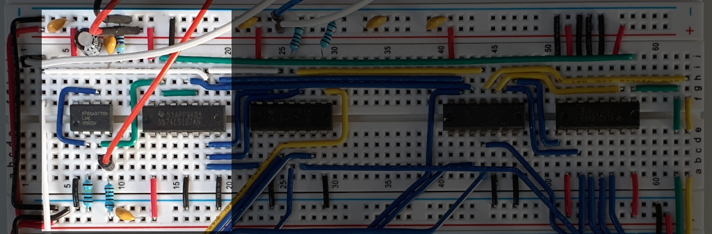
Serial clock
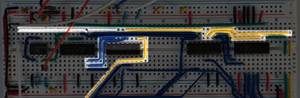
There are actually three separate clock circuits here, though they are all syncronised:
- the system clock (in white). In this implementation this is just a standard Ben Eater-style clock;
- the internal clock used by the ROM->RAM copy circuit; and
- the serial clock connected to the clock input of the ROM chip
Initially, only the system clock will be ticking. The other two are disconnected by the tri-state buffers in the 74HCT125 chip, and pulled low with pull-down resistors (see 'Problems' below for why it wasn't a great idea to use pull-down resistors for the internal clock here).
Since we've connected the Q line from the JK
flip-flop to the enable input of the two buffers, as soon as the flipflop goes high (one clock cycle
after the reset line goes high) we will connect both the internal and serial clocks to the system
one, and they will all start ticking together.
The reason that we separate the serial clock from the internal one like this is so that we can leave the serial clock disconnected from the internal clock when we're done. This will allow other components in the CPU to use the ROM chip (for example, if we want to support flashing the ROM while the system is running, which is perfectly feasible). If we left the serial and internal clocks connected then anyone driving the serial clock would also be clocking this ROM copy circuit while the system is running, which we definitely don't want.
Bit counter
** Note ** All the counter chips in this circuit are placed upside-down (pin 1 is the top right, not the bottom left as usual. This was because it made the routing much simpler (the outputs always flow down).
This counter is responsible for counting from 0-7 repeatedly while the circuit is running. Unfortunately, I didn't have any 3-bit counters, but I did have lots of 4-bit 74HCT161 counters. This doesn't really matter, since we can just use the bottom three bits to cycle from 0-7. Before looking at the detail of how this counter is set up, however, it's useful to think about what we're going to use it for:
- we need to know when the ROM is going to read the 7th and 8th bits on the MOSI line on the next clock tick, so we can set it high accordingly;
- we need to know when we're going to wrap around to zero on the next clock cycle, so we can enable the state counter to advance at the same time;
- we need to know when the shift register has clocked in all 8 bits, so we can set the RAM's
WEline low to store the byte we just clocked out of the ROM - we need to know when it's safe to advance the RAM address counters by one, after we've safely
set
WEhigh again, so we don't change the address lines while we're writing
The first three of these suggest that we actually want the bit counter to count 1 cycle earlier than the serial clock, since all of them deal with needing to know what's going to happen on the next cycle. Fortunately, this is exactly the behaviour that we get if we feed the serial clock directly into the counter:
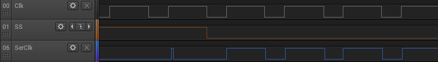
The trace above is from a logic analyser tracing the main system clock (Clk), serial clk
(SerClk), and CS lines in our circuit. As we can see, because the CS line goes low on the
trailing edge of the clock cycle, the next rising edge on SerClk will clock in bit 0 to the ROM,
and at the same time increment the counter to 1. On the following rising edge, we'll clock in bit 1,
and increment the counter to 2, etc.
In reality, however, this isn't exactly what I ended up doing here. It turns out that it's really useful later on to have the counter count only half a cycle earlier, not a full one (see 'Memory Signals' below for why). To do this, we can simply invert the clock signal before passing it into the counter:
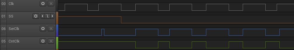
Here, the green line is the inverted clock that's passed to the bit counter. Now, rather than going high immediately at the start of the first cycle, it goes high half-way through each cycle, giving us the half-cycle delay we want. This means that the counter will be wrong for the first half of each cycle, but that still gives us plenty of time to settle down before the next cycle at the clock rates we'll be using.
Returning to our list of the counter's uses above, we can handle #2 quite naturally as a consequence
of this being a 4-bit counter, not a 3-bit one. We want to advance the state counter by one every
time the bit counter rolls around to zero. Since we're counting half a cycle in advance of the
clock, we can simply tie bit 4 of the bit counter to the enable line on the state counter: when
we reach the second half of the cycle for bit 7 the counter will advance to 8 (1000), enabling the
state counter, which will advance on the next clock cycle. We do the same thing for the address
counters, too.
Of course, now we're relying on the value of the 4th bit going high every 8 cycles, we can no longer
just let the counter count to 15 and reset to zero (if we do that, bit 4 will only go high every
second byte, which would be a problem). Instead, we want to reset the counter after 8 cycles.
Fortunately, the 74LS161 allows us to syncronously set its value, by setting the
SPE input low. The counter will then read in the
values on the P0-P3 inputs on the next clock cycle. We simply tie
SPE to the inverse of the Q3 output.
Since we're using the bottom 3 bits to indicate the current bit, we need the value following 1000
to be 0001, so we get the following counting cycle:
0000 - 0
0001 - 1
0010 - 2
0011 - 3
0100 - 4
0101 - 5
0110 - 6
0111 - 7
1000 - 0
0001 - 1
...
State counter and demux
The state counter keeps track of which of the 5 states (command, addr0, addr1, data or finished)
we're in. This has the usual green reset line to
initialise it to zero on startup.
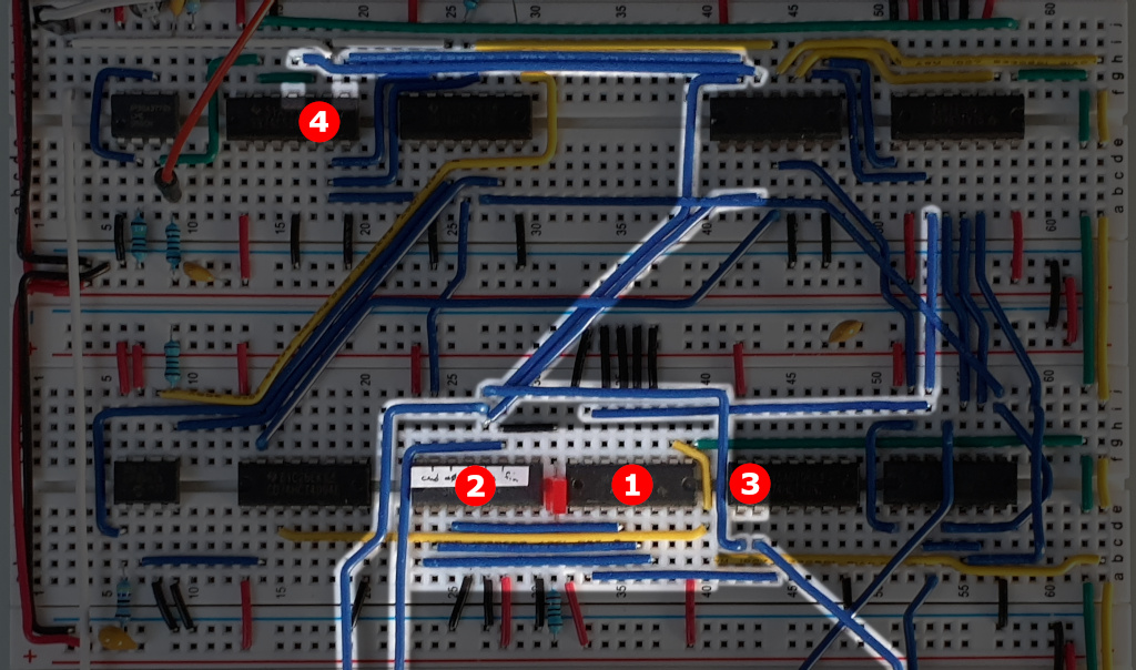
The 74LS161 ❶ counter has two enable inputs, both of which must be high for the counter to advance. We have two conditions that must be met for the state to advance:
- bit 4 of the bit counter output must be high, indicating we're on the last bit of the current byte; and
- if we're in the data state, we don't advance at all until the address counter reaches 216.
We can get this effect by tying one enable line (PE) to bit 4 of the bit counter, and the other
to a line that's high only when the current counter value is 3 and the address bits are all 1
(see below).
Since we need to know the current state value in a few places, and using the binary encoding of the
count is unwieldly, we use a 74LS138 3-8 line
demux ❷ to get 8 individual lines that go low on the corresponding counter value. We take value from
this in several places, but of most interest here is that we feed the Q3 output, which is low
whenever the state is data, and feed it to the 74LS32 quad-OR chip ❸ next to the state counter.
The other input to this comes from the address counter, and will be high iff all 16 address bits are
high (see "Address counters" below for how we work this out). This gives us the second enable input:
it will be high whenever the data line is high (i.e. in any state except data), or when we're on
the last byte.
The final part of note here is the connection to the JK flipflop ❹, which is how we terminate the
copying process. The J and K inputs to the flipflop are tied to finished state line and its
inverse respectively. On startup, the state counter will be initialised to zero, so the demux will
have command low, and all other bits high. This gives us J=1, K=0 on startup. In a JK flipflop
this combo will set the value to 1 on the first clock cycle after the reset line goes high. J
and K will keep these values until the state reaches finished, at which point they swap and we
have J=0, K=1. This will clear the flipflop on the next cycle, which sets the control inputs to
the buffer chip to high, detaching the circuit from the clock and the ROM input lines, effectively
terminating the copy. Since the yellow circuit clock isn't ticking any more, the state will remain
at finished until power off, or a manual reset.
The inverted finished state value is also what we can use as the reset line for the rest of the CPU: it will start off low on powerup, and go high only after all the ROM copying is complete.
Sending the READ command
At this point, we have everything that we need to send the READ command to the ROM chip. As we saw
in the excerpt from the datasheet above, we do this by sending 3 bytes: 3 (indicating the READ
command), then the high address byte, then the low address bytes.
Now, we're fortunate that we're only ever going to want to read the entire ROM chip, so our address
is always going to be 0, so we can really simplify generating the MOSI line: it's always low,
apart from when we're sending bits 6 and 7 of the first byte.
We could get this behaviour by ANDing the inverse of the command line from the state demux (which
would be high only when we're sending the first byte) with bits 1 and 2 of the bit counter output
(which would be high only when the bit counter value was 110 or 111). This requires an
inverter and two AND gates, however, and there's a simpler way. Recall that we said above that we
wanted to leave all the inputs to the ROM chip disconnected when the power-on copy circuit had
completed. If we tie the command state line ❶ to the enable input of one of the spare buffers on the
74HCT125 chip, and pass BIT1 AND BIT2 ❷ to the data line of the buffer, and connect the output of
the buffer to the MOSI line of the ROM chip ❸, then we'll be driving the MOSI line high only when
both command is low and bits 1 and 2 are high, which is exactly what we want. The rest of the time
(during the addr0, addr1, data and finished states) the MOSI line is left disconnected,
and pulled to ground by a 1KΩ resistor.
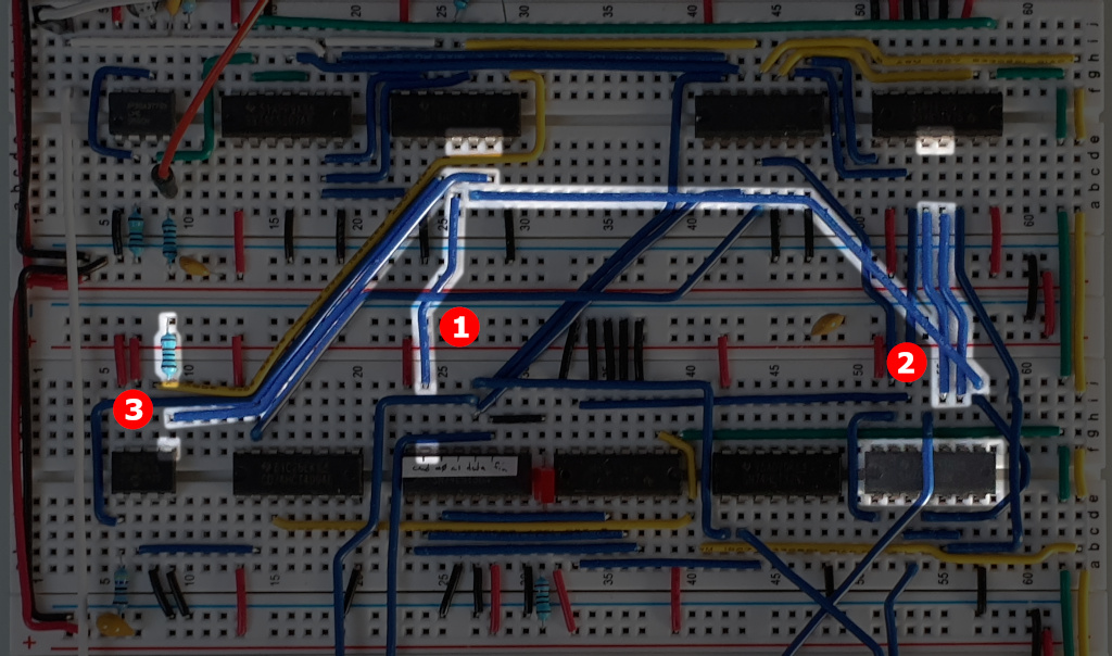
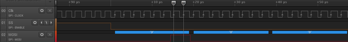
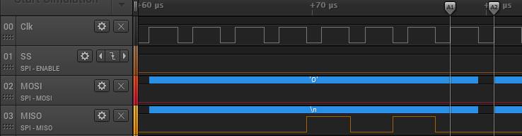
Putting all this together, the following trace shows the behaviour we want. The A1 and A2
markers show the point at which the ROM will snap the value of bits 6 and 7. The numbers in blue
above the MOSI line show the logic probe's decoding of the SPI protocol values, confirming that we
send 3 as the command, then 0 for both address bytes:
ROM and shift register
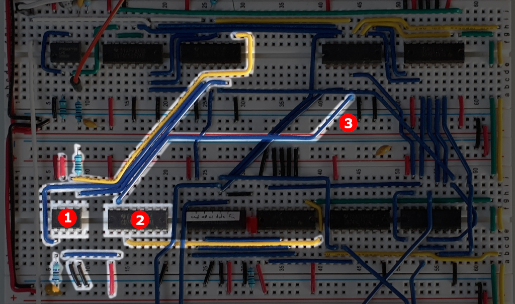
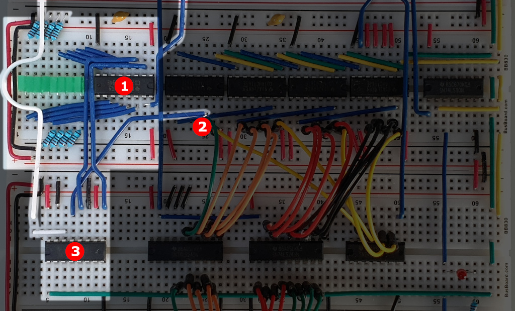
Now that we have everything in place to send the read command to the ROM ❶, we need to look at what we do with the data that comes out. Our RAM chip has an 8-bit parallel data interface, and the serial ROM has a 1-bit serial output. To bridge these two we use a 74HCT4094 shift register ❷.
First, the inputs to the ROM. All three inputs are connected to the 74LS125 buffer chip, so that they can disconnect once copying is finished, and leave the inputs in a high-impedance state, so other parts of the system can drive the ROM:
CSis controlled by the output of the JK flip-flop. When the flip-flop output is lowCSwill be tied to ground, and the ROM is active. When the flip-flop is high (during the initial startup delay, or after copying finishes) then the 4KΩ pullup resistor keeps the chip deactivated.- the
MOSIline (the control input to the ROM chip) is fed from the output of bits 1 and 2 of the bit counter (see 'Sending the READ command' above) - the clock input is connected to the system clock
The 25LC512 has two other inputs: a hold input,
which temporarily pauses the current command so another chip sharing the same SPI bus can use it,
and a wp write-protection line. We won't be using
the hold feature, so we tie that line to 5V. We tie
wp low, so that we don't accidentally write to the
chip if we make a mistake in the input signal.
The ROM chip only has one output (the MISO line). We tie this directly to the serial input of the
shift register. Note that this output is in a high-impedance state whenever CS is high, so we should really have a pull-down or
pull-up resistor here, so that the line doesn't float, but I didn't here, and it didn't affect the
working of the circuit.
The spec says that the ROM chip will start clocking out the data 1 bit at a time, starting with the first falling edge after the end of the address, and it will continue to clock sequential bits out as long as the clock runs. This means that we can basically ignore the ROM chip after this, and the shift register will always give us a view of the most recent 8 bits that we clocked out of the ROM chip. We just need to make sure that we write the output of the shift register to RAM on byte boundaries, which we'll handle below.
The 74HCT4094 has one other nice feature: we can disable the output of the the 8 parallel output
bits, putting them into a high-impedance state, using the OE input. In a simple setup in which one
ROM chip is connected to one RAM chip this lets us avoid the need for an extra buffer chip to
release the data lines once copying has finished and leave them free for the rest of the system to
use. In this simple setup I've connected this to the inverse of the data state line ❸, so that the
register outputs only during the data phase of the operation.
Address counters
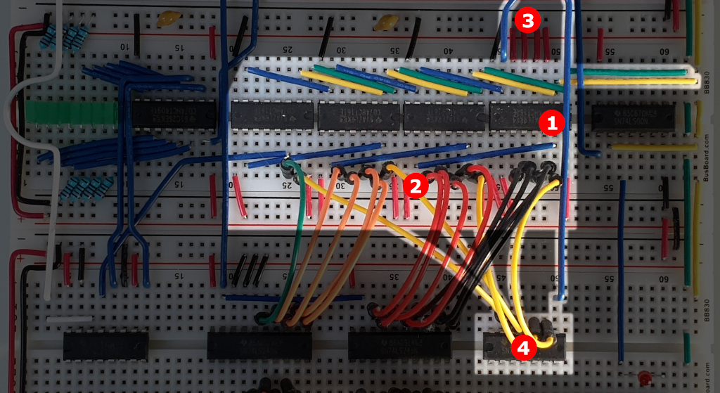
The address counter setup is pretty simple. All these have to do is to count from 0 to 216-1, incrementing once every 8 bits during the data phase of the copy.
Since these are 4-bit counters, and we need a 16-bit counter, we need to chain them together. The
TC pin ❶ on the 74HCT4094 is designed to allow easy chaining of multiple counters. This pin goes
high only when the counter value is 15 (i.e. 1111). By connecting this pin on counter 0 to the TE enable
pin ❷ of counter 1, and TC on counter 1 to TE on counter 2, etc., each successive counter will
count up by one only when the previous counter is at its maximum value. Counter 1 will only count
once every 16 cycles of counter 0, and counter 2 once every 16 cycles of counter 1, etc.
We control the counting behaviour of counter 0 by connecting its PE enable input to bit 3 of the
bit counter, which is high once every 8 bits, though since we only want to count during the data
phase, we first AND bit 3 with the inverse of the data output from the state demux ❸.
Note that I unnecessarily tied all the counters' PE inputs together. In theory I could have tied
all but counter 0's PE inputs high, since they would still be controlled by their TE inputs, but
it's harmless (just extra unnecessary wires to cut).
The only remaining point of interest here is how we stop the counting. Recall from the 'State
counter' section above that we pause the state counter when we're in the data state until we
reach address 216-1. We construct the signal that signifies reaching that address by
feeding all 4 counters' TC pins into a 74LS21
4-input AND gate ❹. Since the TC output is high only when the counter is at value 1111 this gives
us a line that's high only when the counter is at 1111 1111 1111 1111.
Writing to RAM
The final functional part of the circuit handles connecting the address lines to RAM, and
controlling the RAM's WE line to write data.
Connecting the address lines up is simple. We take each of the Q outputs from the counters and
wire them to a pair of 74LS245 line drivers, so
that we can disconnect them when the copy is finished, and leave the address lines free for the rest
of the computer to use. The '245 chip is somewhat overkill, as it is bidirectional and we're only
ever going to use it in one direction, but I had lots of them around, and the pin layout is very
convenient. We tie the DIR pin to ground, which connects the B pins on the north side of the
chip to the A pins on the south.
The outputs of the line drivers are connected to the RAM chip's address inputs (note that the order
that we connect the address pins really doesn't matter, as long as we're consistent). In this case
I'm using an
AS6C6264
8KB RAM in the test I photographed, so we only use 13 address lines. This means that the memory will
be overwritten 8 times, and end up containing the top 8KB of the ROM. In the final circuit I intend
to take the top 3 address bits, feed them into a 74LS138 3-8 demux, with the outputs wired to the
CE inputs of 8 different RAM chips, so that each in
turn gets 8KB of ROM.
The data inputs of the RAM can be directly connected up to the QP outputs of the shift register,
since that has tri-state outputs. I haven't shown that connection here as I used ribbon wires that
obscured the chips beneath.
The final control for the RAM is the WE line. This
must go low when the shift register contains the 8 bits we want to write, and the address lines
contain the correct address. It's important to note that this RAM (and most SRAM these days) is not
syncronous. There is no clock line to control when the inputs are snapped. In particular, we have
to make sure that the address lines stay stable for the entire time that WE is low. If they aren't, and change even slightly while
it's low we could end up writing to the wrong address. It's less important that the data line is
stable for the entire time, so long as it is stable for at least 25ns before
WE goes high again (see the spec linked above for
these TDW and TDH timing values).
The diagram above shows the period during which it's safe for WE to be low. Before A1 we won't have snapped the last
bit into the shift register, and at A2 the data will change to include the first bit of the next
byte, and no longer be correct.
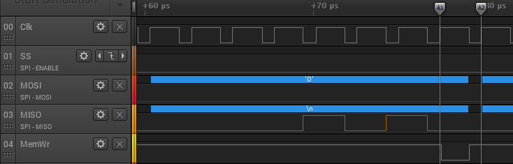
My first implementations used a non-inverted count clock, with the bit counter advancing exactly
one cycle ahead of the data. In theory, with this I could simply tie WE to the inverse of the bit3 output of the bit
counter, which is high exactly when we're in the period A1-A2 in the diagram above. The problem
here was that I ran into timing issues. In theory, bit3 goes low exactly at A2, at the same
time as the data lines change to refect the new bit, but in practice there's propagation delay to
worry about, and the delay of the inverter on the bit3 line was sometimes just enough that WE stayed low after the data had changed. I tried
AND'ing the bit3 value with the clock, so that WE
stayed low only during the first half of the cycle, but this ran into the same problem: at the end
of the interval the clock line would go high a few nanoseconds before bit3 went low, causing WE to blip low again just after the data had changed:
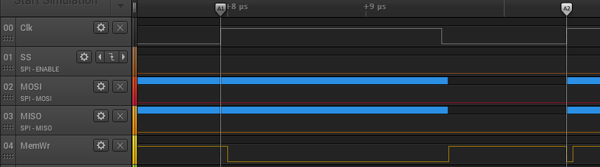
I ended up settling on the approach I described above, where the bit count advances only half a cycle
early, and used bit0 & bit1 & bit2 & clk as the
input to the WE pin. With this, I get the desired
effect, with writes happening only during the first half of the safe window, and no blips at the
end:
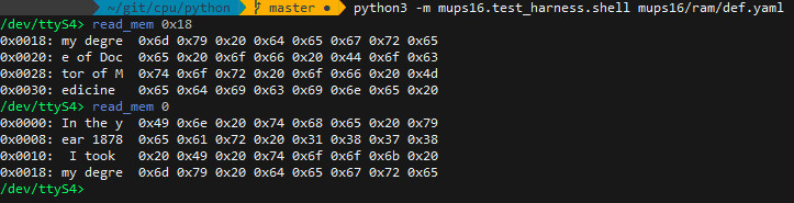
And, with this in place, copying works! We can hook up an Arduino to the address and data lines of the RAM and read the contents once the copying circuit has reached the finished state and disconnected itself:
Progress bar
One final part which has no functional value, but which adds the all-important blinkenlights, is the
progress bar display which shows how far through the copy we are. For this we use another
74HCT4094 shift register ❶ that's initialised to
zero, and which shifts in the value 1 every 8KB.
Advancing the register every 8KB is quite simple. We need a line that will go high exactly once
every 8192 bytes, which we can tie to the clock input of the register. Counter 3 has almost exactly
what we want in output Q1 ❷, which toggles every 4KB: it's low for 4KB, then high for 4KB, giving us
one low-high transition every 8KB. This is almost perfect. The only minor problem is that the count
is offset by 4KB: the low-high transitions happen after 4KB, 12KB, 20KB, etc., instead of 8KB, 16KB,
24KB etc. In practice, this doesn't really matter, and isn't noticeable.
Unfortunately, initialising the shift register to zero isn't quite as trivial as it sounds. There is
no reset pin on a 74HCT4094, so we don't have any way to directly set it to zero. The only way to do
this is to shift in 0 at least 8 times. To do this, we make use of a
74LS157 quad 2-1 multiplexer ❸. By tying the green
reset line to the selection bit of the mux we can
choose between the input values 0 during reset, and 1 during running of the circuit, and connect
the output to the D pin of the register. We use a second unit of the mux to choose between the
white system clock line during reset (to ensure that we clock the 0s in as fast as possible, to
clear the register), and the Q1 output from counter3 mentioned above, connected to the CP pin.
Performance
The fastest clock speed I've been able to run this circuit at on breadboards is about 425KHz. I suspect I could significantly improve on that if I ditched the rubbish Elgoo breadboards I started with and replaced them with the BB830 ones, which have given me far less trouble, but for testing 400KHz is fine. At that speed copying 64KB takes almost exactly 1.25 seconds. With a 4MHz system clock the copy would take just under 150ms, which is perfectly acceptable during startup. Even if I have to step down the system clock to well below 4Mhz (and I almost certainly will) we can still run this copy circuit at full speed.
Problems
Mostly, this circuit just worked once I'd sorted out the bit counting. The main problems I still have are:
- I started out using the same Elgoo breadboards I used in my ALU, and I hadn't realised just how bad they were until I finally got my hands on some BB830 boards, and suddenly all my random power problems and bad connections went away. I should have replaced the three Elgoo ones used here, but I was lazy, and as a result I still see transient power issues, especially when running above 400KHz
- I used pull-down resistors on the internal clock line. This was a poor choice, as TTL chips
already have pull-up resistors on their inputs, and with 8 TTL chips connected to the clock line
the pull-up resistors are strong enough to drag the resting voltage of the clock line to nearly
0.6V, which is dangerously close to the 0.8V threshold for TTL inputs to be considered low. I
had problems with transient voltage spikes happening at the time that the reset line went high
and every chip in the circuit came out of reset, which caused phantom clock ticks (you can see
these in the logic analyser traces in the 'Bit counter' section). Since these didn't happen
while
CSwas low they were ignored, but still not ideal.