Version 1.1 of the μcode address generator
Posted on Fri 19 July 2024 in MUPS16
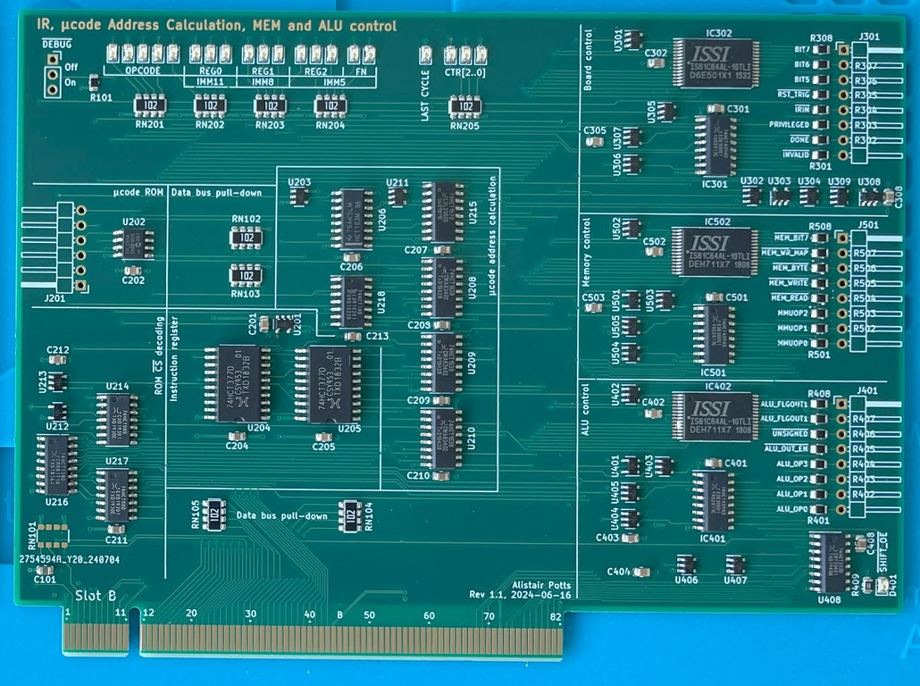
Since the first version of the μcode address generator had a few issues, I re-worked it to fix them, and while I was at it I let a bit of feature-creep happen. The 1.1 revision of the board has quite a lot more functionality than the 1.0 one:
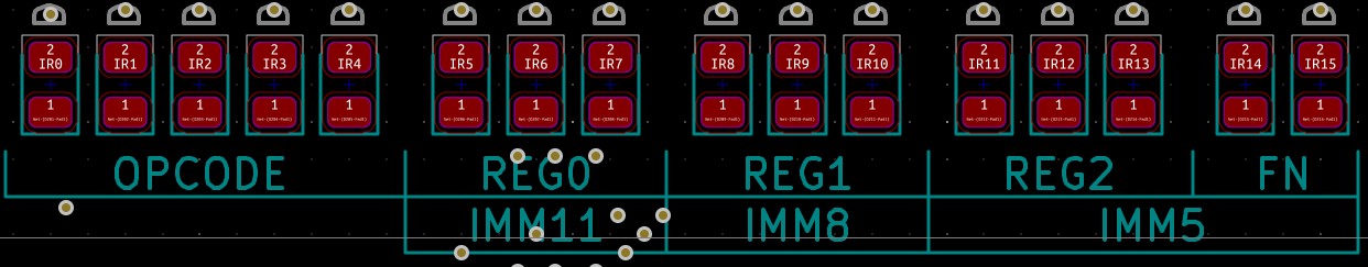
- it still does the translation from opcode to μcode address, and has the instruction register itself
- it now has the ROM chip that contains all the μcode, along with pin headers for flashing and debugging it
- I added three of the six RAM chips in the control unit to this board:
- one containing the μcode for the control unit itself (things like the done, irin, invalid bits etc.
- one with the memory and MMU control lines (mem_rd, mem_wr, etc.)
- one with the ALU control lines
- lots more LEDs!
To fit all this, I sized it up to the same size as the PC/IMM board:
I had a few issues with the soldering, all of which I think were down to the new solder paste I was using, which is a Chipquik low-temperature solder. I thought it would be an improvement, as it melts at 165°C, so I could almost reflow the solder on the pre-heater of my soldering station. It does melt significantly more easily than the old one, but it seems to have much lower surface tension, and produces far more tiny solder balls that cause infuriating bridges. I think I'll go back to the old version next time.
Another annoyance that I only noticed after I'd soldered everything together: all the LEDs for the IR are backwards: bit 0 is at the left instead of the right, and, to make it more confusing, I had the silk-screen the right way round, so nothing matches:
This obviously won't affect correctness of operation, but it's very annoying, and makes it hard to see at a glance what they current op is.
Once everything was assembled, I initially struggled to get anything to work properly via the test board. Even simple things like loading a value into ir didn't do anything. This turned out to be an embarassingly simple problem: I'd installed the test board into the wrong type of slot on the backplane, so it couldn't actually drive the signals for the μcode generator:
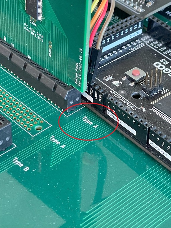
(A slots are for testing things on the memory bus, so they have a full complement of physaddr connections in place of a bunch of the control lines that are internal to the control unit). Once I put both boards into B slots, things started to work.
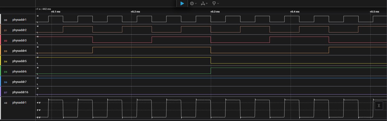
Testing the basics in isolation via the test board and some Python unit tests seemed to go fine, so I plugged everything in, powered it on, and ran the clock for 600,000 cycles to let the reset board generate the SPI->RAM copy signals. This didn't go so well. I had the logic analyser recording the SPI signals and the ramcs0 and we line of the first RAM chip, and it appeared that the initial 1 KB copied correctly, with we going low every 8 bits for the first 1KB then stopping, which is exactly what we want. However, the ramcs0 line was sporadically going low later on in the copy sequence (somewhere in the middle of copying the fourth KB), which re-enables the RAM chip, and results in bits of the fourth RAM chip (the memory control one) being written into the first:
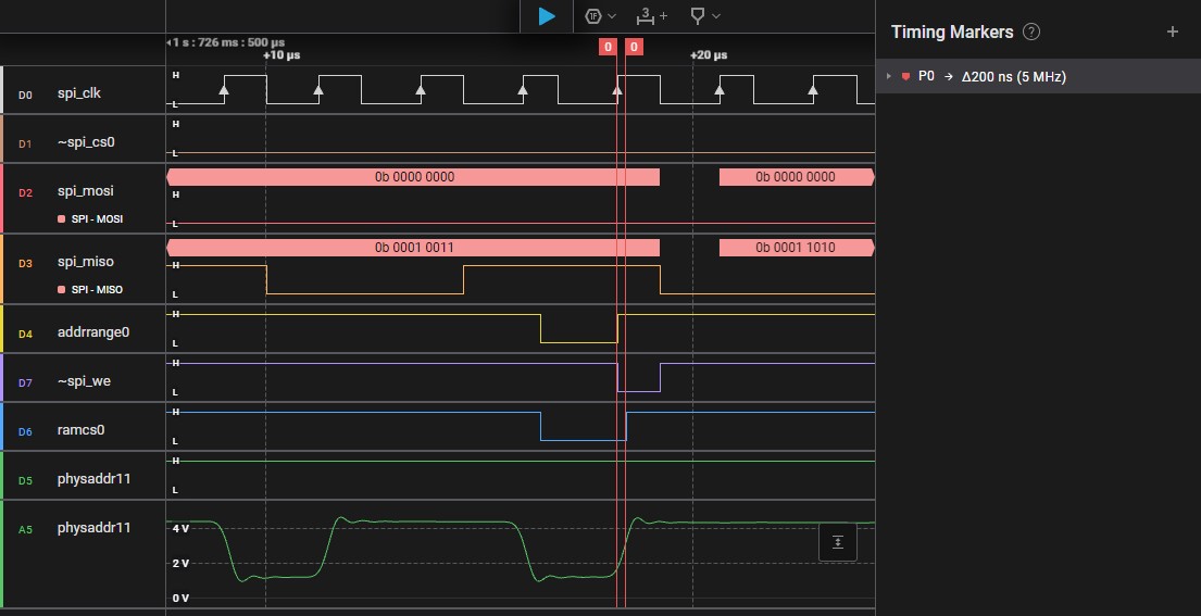
These spikes happened at different points in the byte, but at least a few of them overlapped with the we line going low for long enough to cause a write to RAM (in the example above the overlap is about 200ns, which is way above the 12ns threshold for a write in the RAM chips I'm using.
Digging further, it seemed to be coming from instability in the physaddr lines that the reset board controls during startup. If I removed the μcode generator board and just traced a few lines from physaddr during the reset period then things looked good:
This only shows the bottom 7 bits and one high bit, but the pattern is clear. As soon as the μcode board was reinserted in its slot in the backplane, the address lines went wonky:
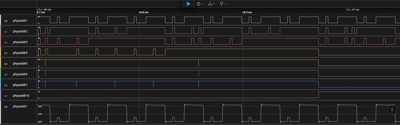
There was clearly something interfering with the same frequency as the clock (white line is physaddr1, which ticks every two clocks). The voltage is pulled to about 1v each time (either up from 0 or down from about 4.3V, which is itself a little lower than expected).
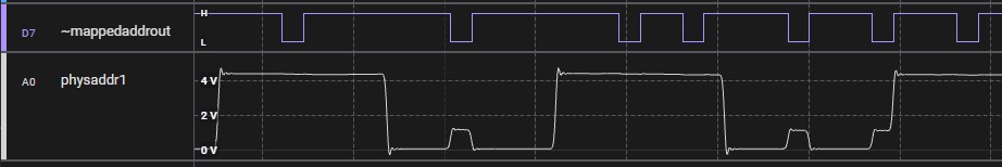
In the end, the answer was embarassingly simple once I noticed it. The issue is the way that the RAM is written during the reset period. Each RAM chip only has one set of 8 data lines. During a read the RAM chip drives these lines, and they are connected either directly to control signals, or to some combinatorial logic. During a write, however, the data lines are driven by a shift register that is accumulating 8 bits at a time from the serial ROM chip. The problem is that these data lines are still connected to the control lines while the shift register is driving them. For most, this isn't an issue, as most parts of the CPU ignore their control lines during reset. The MMU, unfortunately, does not, and so when we get to the fourth KB of ROM and the shift register for the memory part of the control unit kicks in, we start asserting all sorts of bit patterns onto the memory control lines as bits are shifted in, and one of those (0b001 on the mmuop lines) will cause the MMU to try to drive the physaddr bus with whatever is in the page table RAM. Sure enough, probing the relevant line in the MMU shows it triggering exactly when we see the voltage spikes and drops:
The correct solution here is what I should have done in the first place: put a buffer chip between the RAM data lines and the control lines, and tie its oe line to the ctrl_drv line (which is always high during reset). This will decouple the RAM and shift register from the rest of the CPU while they're sorting out the initial writes. In the meantime, however, I managed to hack something together by desoldering the MMU's 3-8 line demux, cutting its active-high enable line that I'd tied to vcc, and then soldering on a write connected to reset instead. That way, the chip is disabled (and outputs all high) during reset.
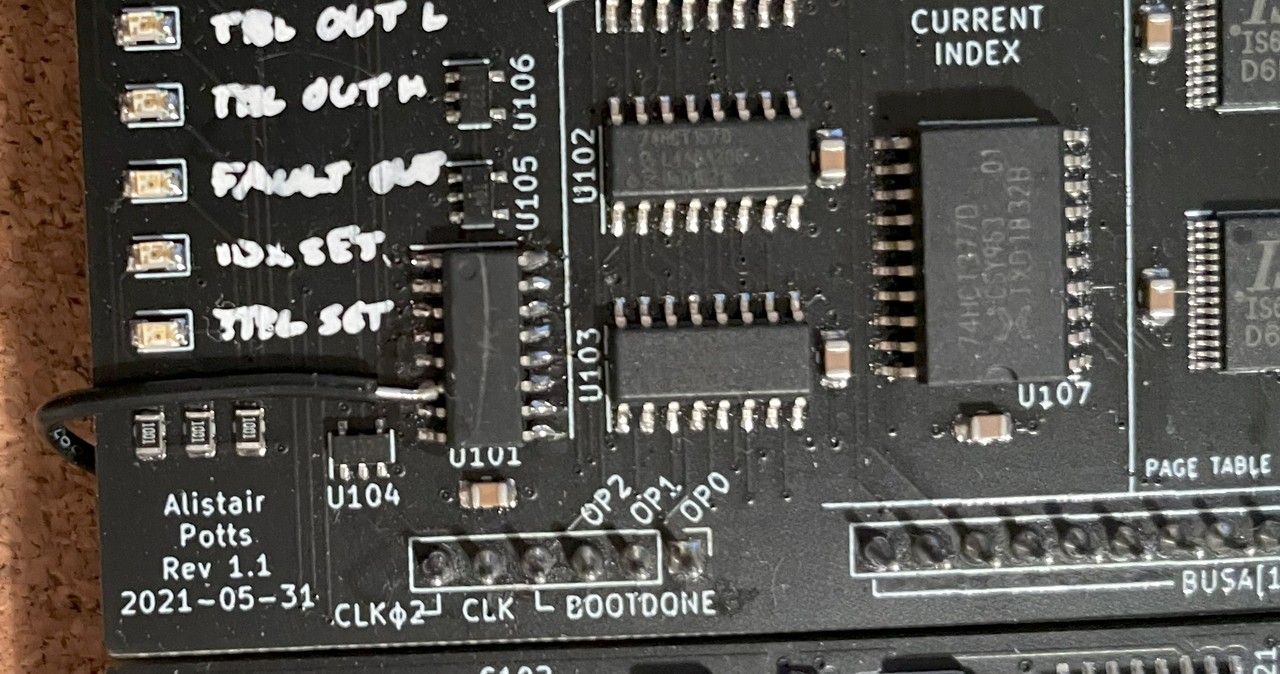
The poor MMU is looking a bit sad between the missed silkscreening of the LED labels and now a big bodge wire, but With that fix in place, the intial ROM->RAM copying seems to be working now. Onwards...
Remaining Bugs
- silkscreen for right-angled pin headers is wrong (offset by about 2.5mm). I think it's designed for headers where the bend is on the board side of the plastic boxes.
- silkscreen for SPI pin headers is completely missing pin names
- green LEDs need to be using 4.7kΩ resistor networks, not 1kΩ. They are way too bright.
- if invalid is set we get stuck in an infinite loop, as the exception unit is not clearing the invalid flag properly (I think because it only clears on done, and done isn't being set for invalid instructions)? Alternatively (and perhaps better?) just set done on all invalid steps. All control lines are forced to safe states by default anyway.
- ctrl_drv does not get forced high on an invalid instruction. It should be forced high on both invalid instructions and privilege errors.