First Control Boards Ordered
Posted on Mon 19 September 2022 in MUPS16
I finally decided to stop tweaking the design of the pieces of the control unit that have been mostly complete for almost a year now, and just send them to be manufactured. There are four new boards here:
- a new lower backplane
- a new tester board to allow an Arduino to read/write all the new lines
- a board containing the instruction register and instruction decode logic
- a board with the program counter and immediate unit
Note that these are not intended to be the final form of any of the components. I'm fully expecting to have to replace them with at least one more revision to work out bugs or design mistakes. This is also why they have very few LEDs to display their state, compared to the other units I've already completed.
Backplane
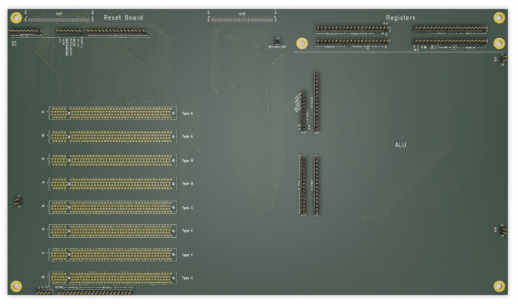
The new lower backplane has the same external connections to the register board and the memory backplane, and space to plug in the ALU, as the previous one did. The main difference is that the area where the old tester board used to plug in flat is now replaced with 8 PCIx16 slots, each with 164 connections, to use for plugging in control unit sub-boards. The idea is that I can split the control unit up into lots of small, and very cheap, plug-in cards that can be iterated on individually, rather than spending a fortune in time and money trying to get the whole unit working correctly on one large, and very dense, board. In theory, once I've debugged the individual parts I could try to convert all the cards into a single board again, so that the whole computer lies flat, as I originally invisaged it. We'll see.
The design of the backplane is pretty simple, since it's mostly the same as the previous one. The complexity comes solely from the challenge of routing signals through the dense forest of through-hole connectors for the PCIx slots. I tried all sorts of ways to make that work with 4 layers, and in the end gave up and threw a bit of money at the problem by making the backplane 6 layers, so that I could have 4 signal layers (on for each row of pins), and the 5v and ground planes. It's a layout that would make an electronics engineer cry thinking about the crosstalk, transmission lines, etc., I imagine, but I'm hoping it'll do for my purposes. So far my agricultural approach to electronics has worked ok.
The pin layouts of the slots in the backplane are not all identical. There are a pair of slots at the top (marked Type A) which have connections that match those on the memory backplane above, so that if necessary I can experiment with new memory-bus-connected components (e.g. display, UART, etc.) on the same backplane). There are 26 currently-unused pins in these slots, for future use.
The Type B slots are intended for control unit cards that still need access to the physaddr bus. Currently, the only one that needs that is the instruction decode card, as that also has the support circuitry to drive the copy the contents of the microcode ROM to RAM. This uses the SPI and address signals generated by the reset unit, so it needs to have connections for the physaddr bus. The second slot is to allow plugging in the tester card for debugging of the instruction decode card. As well as the address bus, this has connections to all other control lines, the A, B and data buses, outputs for the bits of the current instruction word, the current decoded microcode address, and inputs for things like privlege errors, a pending exception flag, etc.
The Type C slots are what most of the control unit will use. These have the same connections as Type B, except that the physaddr pins are replaced by unused_cX, so I have some flexibility to add new intra-board connections. Four of these have already been taken to feed the current exception index (i.e. 0-7 for pending interrupts, 8 for a syscall, 9 for a page fault, etc.).
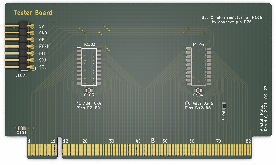
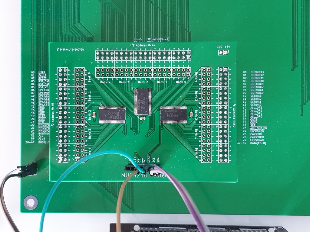
Tester Card
The first plug-in card I made was a new tester, to replace the previous one. The new one has one extra IO expander for a total of 4 (two on each side), each of which has 40 I/O pins, so that the Arduino now has 160 addressible pins, which is exactly enough for the 160 non-power pins on the backplane.
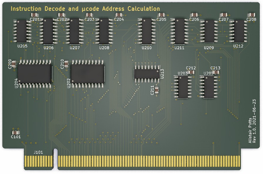
Instruction Decode Card
This card is responsible for two related tasks:
- storing the current instruction word, and using the five opcode and two function bits from it, combined with a cycle counter and exception inputs, to generate the current microcode address, which is output on the ucaddr[0..9] lines. The bottom 11 bits of the instruction word are also made visible on the backplane, as they are needed by the immediate unit in some instructions;
- during startup, using the control signals from the reset board to generate appropriate enable signals for the 8 RAM chips spread around the control unit, so that each is initialised with the appropriate 8KB chunk of the 64KB control ROM.
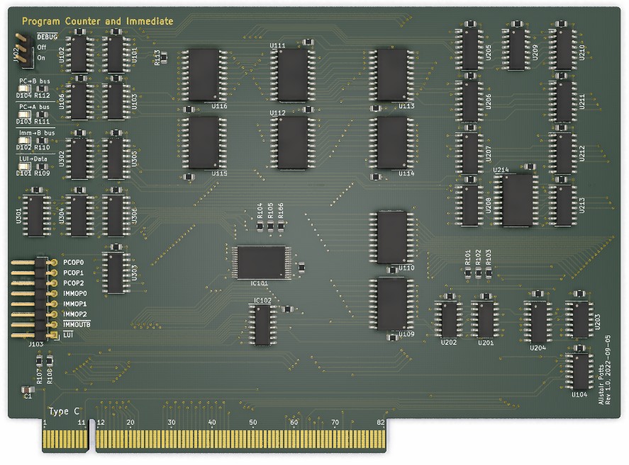
Program Counter and Immediate Card
This card has two separate components of the control unit on it:
- the program counter register
- the immediate unit
The immediate unit is simple enough. It takes the 11 bits of the current instruction word and outputs them either unchanged (for immediate inputs to arithmetic operations), or shifted left by one (for jumps and branch offsets). Outputs can also be zero- or sign-extended. The output from the unit can either go to the A or B buses, or to the program counter (which is why they are on the same card). There's one final small component that's logically tied to the immediate unit, which takes the contents of the A bus and replaces the upper 8 bits with the lower 8 bits of the instruction word, writing the output to the data bus. This is used to implement the LUI (load upper immediate) instruction.
The program counter is slightly more complicated. It's addressible like a normal register for reads, but it has a separate 3-bit group of control lines that are used to set it. These have 6 active values:
- 0: unused
- 1: set from immediate unit output. Note that since the maximum number of meaningful bits the immediate unit can output is 12, as there are 11 non-opcode bits in an instruction, and these can be shifted left by one, the upper four bits of the PC are left unchanged. This means that jumps to immediate addresses cannot cross a 4KB address boundary.
- 2: set from the current exception. This just takes the current 4-bit exception index, shifts it left by one, and sets PC to this value, effectively turning the bottom 16 bytes of memory into a jump table for exceptions and interrupts
- 3: set from the data bus. This just copies the contents of the data bus into PC as-is
- 4: set from the data bus, but only iff the eq flag is high. This is used for various condiontal branch instructions
- 5: set from the data bus, but only iff the eq flag is low. This is used for various condiontal branch instructions
- 6: increment the current value by two. This moves the CPU onto the next instruction in sequence.
- 7: noop. The unit has pull-up resistors on the control lines, so this is the safe state that the unit is in when nothing is driving it
The PC is implemented as a bunch of multiplexers to chose between inputs, and four 4-bit settable counters. These can be either set to a 4-bit value on a rising clock edge, or increment the existing value. This lets us implement the increment instruction without needing to feed the value through the ALU. Note that the counters can only increment by one, but we want to increment by two. This would be a problem, except that the design requires that all insructions are 16-bit aligned, so we know that the bottom bit of the PC must always be zero. So, we can just not store it at all, and the counters are holding bits 1-15 of the PC. This means that incrementing them by one increments the PC value by two, as we need.
I'm not entirely happy with the design of the immediate unit and PC. In the current architecture, I think it could have been implemented much more simply by removing the direct connection between the immediate unit and the PC, and using the data bus to connect them. I didn't implement it like that because I had one eye on what would be required to add pipelining in future, in which case not tying up the data bus would improve efficiency, but it did complicate routing the card quite a bit.