It seemed like a good idea at the time
Posted on Thu 20 August 2026 in MUPS16
Sometimes you have what seems like a genius idea that comes back to bite you later. Back in 2022, when I started building the control unit, I had an idea that I thought would both prevent bus contention and simplify debugging.
The Plan
The problem was that when I was thinking about how the control unit for the CPU would work, I knew I was going to be using ROM to hold control signals for each component, indexed based on the current instruction's opcode and the cycle number, but I was struggling with working out the signal timings.
As an example, take the ALU: it has a control line (ALU_OUTPUT) that comes straight out of ROM and into the OE input of the bus drivers connected to the DATA bus, meaning that as soon as the ROM outputs change in a step that uses the ALU, the ALU will start driving the DATA bus. The memory board, however, can also drive the DATA bus, and on that board, the drivers aren't directly wired to a control signal from ROM, as they have to go through some address decoding to see if the signals are intended for ROM, RAM or memory-mapped devices. This adds a reasonable chunk (tens of nanoseconds) to the time before the bus drivers can change. This would mean that if we had a microcode stage that read from memory that was immediately followed by one that uses the ALU, it's likely that the ALU would start driving the DATA bus quite some time before the memory unit released it.
The problem got worse when I thought about it a bit more, too: the output of the ROM is unstable for some time when the address lines are changing. That means that when the cycle counter increments as an instruction executes, and the microcode address updates, the outputs may be effectively random for some time (up to 10ns for the output to settle for the IS61C64AL-10 chips I use, plus whatever extra is added by the address construction circuitry, which would be tens of ns more) and we can't really reason anything about who is driving the buses during that period.
So, my genius idea to solve this: gate all the outputs from the control unit with latches, at the end of each cycle, immediately force every board's control signals to a 'safe' value using pull-up resistors, while the control unit gets on with setting up the ROM output for the current cycle. During this period, no-one should be driving any buses. Once the outputs are guaranteed to be stable, we enable the latches, and the new control signals update simultaneously, and all is gloriously well with the world.
As a pleasant side-effect, during the initial period when the drivers are disabled, I could drive any of the control signals myself to debug things.
The way that I implemented this was to split the clock cycle into four parts, and generate two different clock signals: a 1/4 duty cycle clock (CLK_Q) that was used by the control unit, and a normal 1/2 duty-cycle clock for the rest of the CPU (CLK_H). The output drivers for the control unit were fed the CLK_Q input directly, so that they were disabled while it was high at the start of the cycle, and low for the last 3/4:
Figure 1: The intended control unit clocking, as I imagined it.
The rest of the CPU would then see the control signals from the second quarter of the cycle onwards, which I thought would give enough time for them to settle their outputs before the end of the cycle.
This was the design that I implemented for all versions of the control unit up to now. You can see the '541 output drivers on each of the little control memory boards:
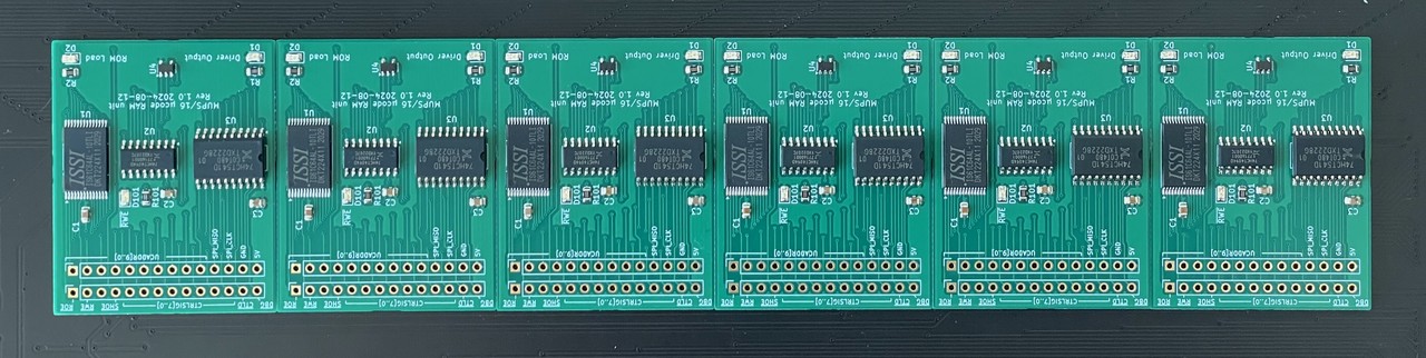
It works. Mostly. The debugging support has been great: I have found a lot of problems by hooking up an Arduino snooping the main bus and control lines on every cycle and looking for unexpected values. I haven't seen any issues with bus contention either. So, what's wrong?
The Problem
The first sign that there was an issue was this trace I captured from the ALU, completely by accident, while debugging an unrelated clock issue:
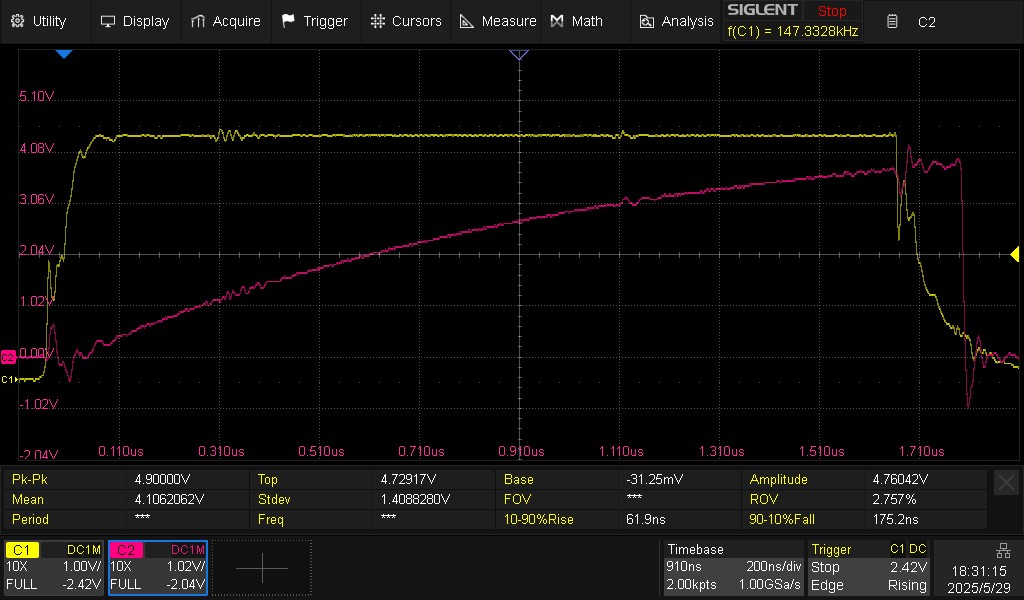
Figure 2: One of the ALU control lines in purple, and the CLK_Q signal in yellow
That purple control line is meant to snap up to 5V as soon as the clock goes high. Instead, it slowly drifts up there over the whole period that the clock is high, eventually reaching about 4V by the time that the clock goes low again and the control line is re-asserted. There are two things wrong here: firstly, that signal is drifting through the HCT logic's undefined 0.8V - 2.0V window for nearly a third of the time that the clock is high, meaning we can't really be sure about what the ALU is going to be doing during that period, invalidating the whole safety argument. Secondly, look at the clock frequency at the top of the screen: 147KHz. This was captured using a breadboard clock running at about 1/25th of the target speed of 4MHz, and the signal only just made it to 4v in that time.
The problem is the pull-up resistors. I use 10KΩ, which is evidently far too weak. So, easy solution: try stronger pull-ups. Well, I at least had the sense to work out whether that might work before I wasted an afternoon desoldering lots of resistors off the control unit. Short answer, no: at 1KΩ it would still take about 50-100ns to reach 2.0V (with lots of hand-waving since I had no real idea what the capacitance of all the traces and connectors on my backplane were).
The second problem is that I've started to look in detail at what it would take to get to 4MHz, and I just can't make the numbers add up when I am spending a quarter of the 250ns for each clock at 4MHz with most of the CPU idle. In particular, I can't get the register -> ALU -> DATA -> register path below 212ns in the worst case even with AHCT/ACT parts. If I could reduce the 62.5ns I'm spending each cycle on decoding it would just fit. Time to get my thinking cap on.